Naura is clearly hiding its progress in advanced node tools. I’m pretty sure that all the 8 inch tools have 12 inch versions. It’s more useful to look at patents than websites at this point.As @tphuang and many other mentioned before, Lithography machine does not seem to be the constraints which is preventing expansion of 7nm++ Fab in Mainland. Is it the Etching and Deposition equipments by AMAT & Lam? AFAIK Etching equipments are not a problem for SMIC since AMEC have a good portfolio into 5nm++ Etching equipments. But when it comes to Deposition tools, I looked at Naura portfolio and most of their IC Deposition tools are for like 6-8 in Wafer. They cant possibly be used for 12in Wafer used to manufacture 7nm++ Chips by SMIC
Also anyone knows what's the progress of HuaHong 14nm FinFet? I still think it is of paramount importance that HuaHong also becomes as competitive as SMIC. The Chinese government should put their focus on HuaHong. Sometimes I feel like Liang Mong Song should make a final jump to HuaHong to get them upto speed of SMIC before he retires
You are using an out of date browser. It may not display this or other websites correctly.
You should upgrade or use an alternative browser.
You should upgrade or use an alternative browser.
Chinese semiconductor thread II
- Thread starter vincent
- Start date
Guangxin Materials: Plans to raise no more than 300 million yuan in additional capital for a project with an annual output of 50,000 tons of electronic photosensitive materials and supporting materials
Guangxin Materials disclosed a plan to issue stocks to specific targets through a simple procedure. The total amount of funds to be raised in this issuance will not exceed 300 million yuan, and the net amount of funds raised after deducting relevant issuance expenses will be all It is used in a project with an annual output of 50,000 tons of electronic photosensitive materials and supporting materials.
The funds raised from the issuance of shares to specific targets through a simple procedure will continue to be fully used for the 50,000-ton annual output of electronic photosensitive materials and supporting materials project implemented by the company's wholly-owned subsidiary Jiangxi Guangzhen in Longnan City, Jiangxi Province. By building new factories and introducing advanced automated production equipment and high-end technical talents at home and abroad, the company has built Jiangxi Guangzhen into the main production base and intensive centralized production base in South China, which serves as an important layout for the company to base itself in South China and radiate to surrounding markets such as Central and East China.
Guangxin Materials said that after years of research and development and the introduction of technical talents, the company's technical team has mastered the main technologies and production development processes of new photovoltaic materials, photoresists and peripheral supporting materials. At present, the company has regarded new photovoltaic materials and photoresist technology as the second focus of future development. Mastering new photovoltaic materials and photoresist technology and gradually implementing them in industrialization is the company's need to comply with national strategies, industrial upgrading and its own development. It is conducive to the implementation of new businesses and the construction of new profit growth points to achieve long-term sustainable development of the company.
Aixin Semiconductor completed hundreds of millions of yuan in Series B financing
Aixin Semiconductor successfully completed hundreds of millions of yuan in Series B financing. This round of financing was jointly led by Huahai Gimpo and Zhejiang Venture Capital. The original shareholders Shenzhen Venture Capital continued to increase their holdings, and Yangtze River Capital, Cornerstone Capital, and China Merchants Capital invested in the company.Recently, Aixin Semiconductor successfully completed hundreds of millions of yuan in Series B financing. This round of financing was jointly led by Huahai Gimpo and Zhejiang Venture Capital. The original shareholders Shenzhen Venture Capital continued to increase their holdings. Yangtze River Capital, Cornerstone Capital, China Merchants Securities, Skyline Capital, and Hua Venture Capital continued to increase their holdings. Vos participated in this round of investment. Aixin Semiconductor pointed out that this round of financing will effectively support the company's continued R&D investment and product matrix expansion, enhance the batch delivery capabilities of finalized products, provide a solid guarantee for order fulfillment, and further enhance the competition of Aixin Semiconductor's front-end measurement products for wafer manufacturing. force.
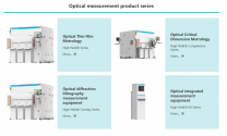
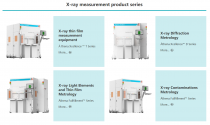
It is reported that Aixin Semiconductor is an enterprise engaged in the research and development, manufacturing and sales of front-end measurement equipment for semiconductor wafer manufacturing. Its products cover optical thin film measurement, optical critical dimension measurement, optical diffraction overlay measurement, optical integration measurement, A series of products and solutions including X-ray film measurement, X-ray material measurement, X-ray composition and surface contamination measurement. Product specifications match international cutting-edge standards and support LOGIC, DRAM and 3D NAND measurement processes. At present, Aixin's products have served leading domestic wafer manufacturers, achieving small-scale mass production and repeat purchase orders for a variety of products.
Aixin Semiconductor is headquartered in Shenzhen, with a R&D and production base of 7,300 square meters, and branches and offices in Shanghai, Wuhan, Chengdu, Beijing, and Hefei.


Naura is clearly hiding its progress in advanced node tools. I’m pretty sure that all the 8 inch tools have 12 inch versions. It’s more useful to look at patents than websites at this point.
Patents provide useful insight for what directions various companies/institutions are exploring, but there's a significant gap between patenting something and commercializing it at scale.
Xiaomi's SoC, looks like it has 2 configs and performance similar to Snapdragon 8 Gen 1+ levelm 的芯片有消息了,消息灵活人士的分享!!目前已经回片,大概在骁龙8+的水平
有两种配置规格,方案1:A715*4+A510*4;方案2:X3+A715+A510;
GPU均为IMG CXT 48-1536,整体为N5工艺,大概是在8+水平,可惜没Modem,预估是通过MTK买M80。
no modem, so have to buy it from someone
Patents provide useful insight for what directions various companies/institutions are exploring, but there's a significant gap between patenting something and commercializing it at scale.
Under a normal situation I would agree with you. But the current situation is really really tense and Chinese entities are looking for breakthroughs by whatever means necessary. In fact I have seen Chinese semiconductor companies making jumps from R&D to commercialization much faster than last past 4 decades.
Yes what’s getting lost here is that given both the opportunity and tensions brought by geopolitical pressures companies have very strong incentives to innovate at greater cost than they normally would. More aggressive R&D pipelines are often riskier and more expensive and that’s often discouraged for the sake of profitability and business viability, but in the current context normal rules don’t apply.Under a normal situation I would agree with you. But the current situation is really really tense and Chinese entities are looking for breakthroughs by whatever means necessary. In fact I have seen Chinese semiconductor companies making jumps from R&D to commercialization much faster than last past 4 decades.
sure, I don't see this as a problem either. I'd be more curious who takes their talent and IP. There are way too many AI GPU startups back in 2022, clearly not all of them were going to survive.
The Chinese government and other technology giants are now investing big in Biren, as they know about its importance to China's chip industry.
antiterror13
Brigadier
What does it mean? Biren will be owned by the govt?The Chinese government and other technology giants are now investing big in Biren, as they know about its importance to China's chip industry.

