Chinese semiconductor thread II

tokenanalyst

Brigadier
Registered Member

Analysis of effective refractive index of TE 0 mode in extreme ultraviolet grating waveguide.​

Abstract
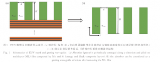
The imaging phenomena in extreme ultraviolet (EUV) lithography must be elaborated from more than one perspective. Traditionally, previous studies on waveguide methods have considered the cladding electric field distribution of the absorber as an evanescent field, which is similar to a single parallel-plate waveguide. However, these studies ignore the periodicity of the absorbers. In this study, the absorber of the EUV lithography mask is regarded as a grating waveguide. Owing to the periodicity of the absorber, two adjacent periods must affect the field distribution. Therefore, the electric field of the absorber is a linear superposition of the adjacent periodic field distributions. We propose that the electric field distribution in the absorber in the lowest-order transverse electric (TE 0 ) mode is a hyperbolic cosine function cosh(·). We provide the zero-order approximation value n eff,0 of the effective refractive index n eff for the TE 0 mode. To further decrease the relative error of n eff,0 according to the boundary conditions, we derive the eigenvalue equation for the grating waveguide . To obtain a good approximation, we derive an iterative formula of n eff, m and use the iteration method to decrease relative error.
1715613866381.png.

Please, Log in or Register to view URLs content!
 

Wahid145

Junior Member
Registered Member
Interesting more so in that both Samsung and SK Hynix have massive plants in China and in fact actually produce half their DRAM GLOBALLY there IN China which these chips for the P70 almost certainly come from.

If the US refuses export licensing for those factories in the future then what happens? That is world class equipment and infrastructure already set up within China. If they were ever sold off because of US bans . . .
Very valid point. But the best case scenario would be CXMT catching up on the LPDDR5X DRAM manufacturing so China will not have to go through this path and I'm sure they are inching closer to it!
 

tokenanalyst

Brigadier
Registered Member

Jiangsu Huatian integrated circuit wafer level packaging and testing base project factory building is fully capped​


According to news from the Nanjing Municipal Development and Reform Commission on May 9, the Jiangsu Huatian integrated circuit wafer-level packaging and testing base project plant has been fully capped. The 3# factory building of this project has been fully capped, the 1# factory building has been completed, and equipment debugging is in progress. This project is a major provincial project and will lay out internationally leading integrated circuit wafer-level Gold Bump packaging and testing production lines, high-pixel image sensor packaging and testing production lines, and integrated circuit wafer-level packaging and testing production lines.
According to news released by Pukou on May 6, the Huatian Jiangsu wafer-level advanced packaging and testing base project has a total investment of 9.95 billion yuan, covering an area of about 466 acres, and is being constructed in three phases, of which the first phase of the project has started. After completion, the project will have the capacity to produce 700,000 wafer-level packaging of integrated circuits such as Bumping, WLCSP, FO, TSV, and SiP per month.

It is reported that the first phase of the project will start construction in November 2022, and the main factory building will be capped in June 2023, equipment will be brought online in October, and the production process will be completed in December; on October 18, 2023, Huatian Technology (Jiangsu) The first batch of equipment of the company entered the factory and the groundbreaking ceremony of Factory No. 3 was held.

Please, Log in or Register to view URLs content!
 

tokenanalyst

Brigadier
Registered Member

Changdian Technology's (JCET) smart driving application has been fully launched!​


As the world's leading integrated circuit finished product manufacturing and technical service provider, Changdian Technology has been deeply involved in the field of advanced packaging for many years and can provide autonomous driving chip customers with diversified, high-reliability packaging and testing solutions and supporting production capacity. As autonomous driving technology at L3 level and above becomes increasingly mature, the automotive intelligence market has fully entered the 2.0 era. Changdian Technology will continue to provide strong technical support and services to customers in the field of intelligent driving and the entire industry.
Currently, the mainstream autopilot solutions are divided into two types, namely, multi-sensor fusion solutions with lidar as the core, and pure vision solutions with cameras as the mainstay. Lidar has high measurement accuracy, wide range, and high safety. Even in harsh environments, it can more accurately perceive surrounding information, so it has been adopted by most car companies. According to statistics, more than 80% of domestic smart driving companies currently adopt this solution; however, its algorithm iteration speed is relatively long. The purely visual solution mainly collects information through cameras and is relatively low-cost. In model calculations, it also involves fewer sensors and fast algorithm iteration, making it another mainstream solution for autonomous driving.
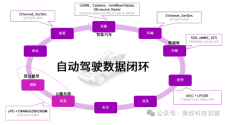
The core of smart cars is realized through a series of closed-loop steps such as data collection, transmission, storage, processing, simulation, training, verification, and deployment. This process involves a large number of different types of chips, and each type of chip also requires specialized chip packaging technology according to its different functions and other requirements.

1715615710773.png


Changdian Technology is at the core of the intelligent driving ecosystem and plays an important role in all aspects. Especially in the fields of intelligent driving sensors and high-performance computing, it cooperates closely with mainstream customers around the world and has many years of experience in mass production of automotive-grade chip packaging. experience. In 2023, Changdian Technology's automotive business revenue will exceed RMB 2 billion, leading the industry in terms of revenue scale and technical capabilities. Changdian Technology can provide one-stop automotive grade chip packaging and testing solutions, including traditional packaging such as QFP, QFN, and BGA, and advanced packaging such as FCBGA, FCCSP, SiP/AiP, POP, 2.5D/3D, etc., fully supporting intelligent computing The processor has high computing power, high reliability, high integration and high bandwidth requirements. In addition, in response to the high energy consumption problem in the process of training large models in the cloud, Changdian Technology has also provided customized packaging solutions to the industry's leading power suppliers, achieving improvements in power distribution, energy efficiency, packaging size, cost and heat dissipation. further improvement.

Please, Log in or Register to view URLs content!
 

Wahid145

Junior Member
Registered Member

GiantPanda

Junior Member
Registered Member
More than just the scanner.
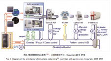
Holistic Lithography Ecosystem
As I see it
View attachment 129524

Optical After Development Inspection-Optical After Etch Inspection


View attachment 129525

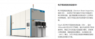
E-BEAM INSPECTION.


View attachment 129526
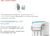
OVERLAY CONTROL


View attachment 129527
COMPUTATIONAL LITHOGRAPHY AND MACHINE MATCHING.


View attachment 129529

It is a very big eco-system and China is being forced to learn and execute every piece of it.

The old saying that what doesn't kill you makes you stronger can't more apt than for China's semicon industry.

They survived the first and deadliest blow, the one that the collective say was "annihilation with no chance of survival". Everything going forward becomes a matter of time.
 

tokenanalyst

Brigadier
Registered Member

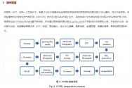
High-Beam-Quality High-Power Vertical-Cavity Surface-Emitting Laser​

Abstract​

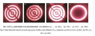
Compared with edge-emitting lasers, vertical-cavity surface-emitting lasers (VCSELs) have superior performance, such as a lower threshold current, single longitudinal-mode output, easy 2D array integration, low power consumption, and low fabrication cost. With the development of large apertures as well as 2D arrays of VCSELs, the output power of VCSELs has been significantly improved, and they are widely used in such fields as optical communication, optical interconnection, and optical information processing. In addition, the applications of VCSEL devices in the consumer field are becoming increasingly extensive, such as LiDAR, distance sensing, autofocusing, 3D sensing, rainbow-mode recognition, air and water quality detection, and virtual reality (VR)/augmented reality (AR)/mixed reality (MR). In recent years, the performances of VCSELs in terms of output power, conversion efficiency, modulation bandwidth, and reliability have improved continuously. However, high-power VCSEL single-tube or array devices are mostly multi-transverse-mode outputs, resulting in poor output beam quality. Therefore, improving device power while obtaining better beam quality in the optical field is a technical challenge that current researchers must solve. In this study, a novel multi-ring cavity structure is used to integrate VCSEL arrays to obtain a better far-field distribution while maintaining a high power output, further expanding the application range of VCSELs in the field of smart devices.

1715633327335.png
1715633287813.png
Please, Log in or Register to view URLs content!
 

Wrought

Junior Member
Registered Member
Unusual conclusion from a Western thinktank, though I suppose this one is European.

Although US export controls are designed to widen Washington’s lead over Beijing in the race for advanced semiconductors, two new studies suggest the crackdown is boomeranging, hurting US business while helping Chinese companies.

Analysis from the New York Federal Reserve
Please, Log in or Register to view URLs content!
the new controls wiped “out $130 billion in market capitalization” for US firms and caused them to “experience a drop in bank lending, profitability, and employment.” Another study from US and Chinese financial experts
Please, Log in or Register to view URLs content!
controls on dual-use tech from 2007-2019 caused Chinese tech manufacturing or assembly firms to produce “more high-quality innovations.”

In short: US pressure appears to be accelerating Chinese innovation while depriving US firms of the revenue needed to keep their lead. Despite this evidence, the Biden Administration defends the chip crackdown and vows to continue expanding the export controls.

Please, Log in or Register to view URLs content!
 
Top