You are using an out of date browser. It may not display this or other websites correctly.
You should upgrade or use an alternative browser.
You should upgrade or use an alternative browser.
Chinese semiconductor thread II
- Thread starter vincent
- Start date
I mean, it has already started with Omnivision.Here it is. The cabbagization of imaging sensors.
Huawei TSV patent.
Huawei’s patent for “a semiconductor packaging and electronic equipment” published
Huawei Technologies Co., Ltd.’s patent for “a semiconductor packaging and electronic equipment” was published. The application publication date is April 5, 2024, and the application publication number is CN117832187A.
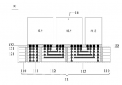
This application provides a semiconductor package and electronic equipment. Wherein, the semiconductor package includes: a back-end process transfer layer, which is divided into at least one interconnection transfer part and at least one redundant transfer part that are arranged independently of each other; any two adjacent transfer parts The first filler is filled between them; each interconnection transfer part is provided with at least one chip electrically connected to the interconnection transfer part. In this semiconductor package, the post-process transfer layer is used to interconnect the chip, which can save TSV-related processes, thereby reducing packaging costs. And because the subsequent process transfer layer is divided into at least one interconnection transfer part and at least one redundant transfer part that are independent of each other, the problems of deformation and excessive residual stress of the subsequent process transfer layer can be alleviated. Reduce the risk of packaging reliability such as cracks in the transfer layer in subsequent processes.

This application provides a semiconductor package and electronic equipment. Wherein, the semiconductor package includes: a back-end process transfer layer, which is divided into at least one interconnection transfer part and at least one redundant transfer part that are arranged independently of each other; any two adjacent transfer parts The first filler is filled between them; each interconnection transfer part is provided with at least one chip electrically connected to the interconnection transfer part. In this semiconductor package, the post-process transfer layer is used to interconnect the chip, which can save TSV-related processes, thereby reducing packaging costs. And because the subsequent process transfer layer is divided into at least one interconnection transfer part and at least one redundant transfer part that are independent of each other, the problems of deformation and excessive residual stress of the subsequent process transfer layer can be alleviated. Reduce the risk of packaging reliability such as cracks in the transfer layer in subsequent processes.
TAIPEI -- Huawei Technologies is building a massive semiconductor equipment research and development center in Shanghai as the Chinese tech titan continues to beef up its chip supply chain to counter a U.S. crackdown.
The center's mission includes building lithography machines, vital equipment for producing cutting-edge chips. Washington's export controls have sharply reduced Huawei's access to this equipment, whose production is dominated by just three companies: ASML of the Netherlands and Japan's Nikon and Canon.
To staff the new center, Huawei is offering salary packages worth up to twice as much as local chipmakers, industry executives and sources briefed on the matter told Nikkei Asia. The company has already hired numerous engineers who have worked with top global chip tool builders like Applied Materials, Lam Research, KLA and ASML, they said, adding that chip industry veterans with more than 15 years of experience at leading chipmakers like TSMC, Intel and Micron are also among recent and potential hires.
Total investment for the the entire R&D base will come to about 12 billion yuan ($1.66 billion), according to the Shanghai government, which listed it as one of the city's top projects for 2024.
The campus covers about 224 football fields in area and is almost twice as big as the company's renowned Ox Horn Campus, a European village-style site in the Chinese city of Dongguan. Like Ox Horn, the Shanghai campus will include trains for commuting between buildings in the campus. When completed, it will be able to accommodate more than 35,000 high-tech workers, according to the People's Government of Qingpu District of Shanghai Municipality.
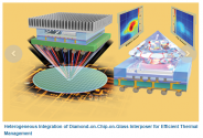
Heterogeneous Integration of Diamond-on-Chip-on-Glass Interposer for Efficient Thermal Management.
School of Electronic Science and Engineering, Xiamen University, Xiamen, China
Huawei Technologies Company Ltd., Shenzhen, China
Xiamen Sky Semiconductor Technology Company Ltd., Xiamen, China
Abstract:
Thermal management poses a critical challenge in the design of modern electronic packages. This letter presents a diamond-on-chip-on-glass interposer (DoCoG) technology that incorporates polycrystalline diamond heat-spreader substrates known for their exceptional thermal conductivity. These diamonds are directly bonded to the back-side of silicon chips on a glass interposer, resulting in markedly enhanced cooling performance. The junction-to-ambient thermal resistance dropped by 28.5% due to the integration of diamond. The creation of such multi-stacked DoCoG integration and efficient cooling necessitates a diamond/chip connection that combines a minimal bonding thermal budget, high working temperature, and low thermal boundary resistance. To address this challenge, the study proposes a low-temperature bonding technique through nanolayer Cu/Au recrystallization. The effects of bonding voids on overall cooling performance were investigated. These results represent significant progress toward universal approaches for the viable integration of high-performance coolers into electronic packages, potentially enabling applications that are currently constrained by thermal limitations in heterogeneous integrations.
Brightcore's listing on the Science and Technology Innovation Board surged 160.3%, with Yuanhe Puhua/Juntong Capital as the major shareholders.
Brite Semiconductor (Shanghai) Co., Ltd. (securities abbreviation: Brite Semiconductor, stock code: 688691) officially landed on the Science and Technology Innovation Board, with an issue price of 19.86 yuan/share and an issue price-to-earnings ratio of 25.12 times. . As of press time, Bright Core shares surged 160.3% to 51.70 yuan per share, with a total market value of 6.204 billion yuan.
It is understood that Canxin Co., Ltd. is an integrated circuit design service company that focuses on providing one-stop chip customization services. The company is positioned in the field of new generation information technology. Since its establishment, it has been committed to providing customers with high-value, differentiated chip design services. Through this research and development, it has formed a comprehensive range of large-scale SoC custom design technology and semiconductor IP development technology as the core. Technical service system.
Juntong Capital is also one of the first domestic private equity investment management institutions focusing on the pan-semiconductor field. As of the end of October 2023, Juntong Capital has invested a total of 4.64 billion yuan in the semiconductor field, and the cumulative number of investments has reached 82. The cumulative investment amount of "Specialized, Special and New" projects has been nearly 1.695 billion yuan, and the cumulative number has been 29. The projects it has invested in have been exited and realized a cash income distribution of over 8 billion yuan. The average DPI of the exited projects has exceeded 7 times, and the average IRR has exceeded 70%.
In recent years, Brightcore has relied on its complete technical system and comprehensive design service capabilities to continuously help customers complete chip design, development, and mass production and launch with high quality, high efficiency, low cost, and low risk.
During the reporting period, Brite Technology successfully taped out more than 450 times, including more than 150 times at 65nm and below logic process nodes, and more than 100 times at specialty process nodes such as BCD, EFLASH, HV, SOI, LCOS, and EEPROM. Second-rate.
According to the report of the Shanghai Integrated Circuit Industry Association, Brite Holdings accounted for 4.9% of the global integrated circuit design services market share in 2021, ranking fifth in the world and second in mainland China, occupying the leading position in the global integrated circuit design service industry competition. important location.
2022 news but NikkeiAsia reposted it with new date in 2024.. LOOL
TAIPEI -- Huawei Technologies is building a massive semiconductor equipment research and development center in Shanghai as the Chinese tech titan continues to beef up its chip supply chain to counter a U.S. crackdown.
The center's mission includes building lithography machines, vital equipment for producing cutting-edge chips. Washington's export controls have sharply reduced Huawei's access to this equipment, whose production is dominated by just three companies: ASML of the Netherlands and Japan's Nikon and Canon.
To staff the new center, Huawei is offering salary packages worth up to twice as much as local chipmakers, industry executives and sources briefed on the matter told Nikkei Asia. The company has already hired numerous engineers who have worked with top global chip tool builders like Applied Materials, Lam Research, KLA and ASML, they said, adding that chip industry veterans with more than 15 years of experience at leading chipmakers like TSMC, Intel and Micron are also among recent and potential hires.
Total investment for the the entire R&D base will come to about 12 billion yuan ($1.66 billion), according to the Shanghai government, which listed it as one of the city's top projects for 2024.
The campus covers about 224 football fields in area and is almost twice as big as the company's renowned Ox Horn Campus, a European village-style site in the Chinese city of Dongguan. Like Ox Horn, the Shanghai campus will include trains for commuting between buildings in the campus. When completed, it will be able to accommodate more than 35,000 high-tech workers, according to the People's Government of Qingpu District of Shanghai Municipality.
this center already started R&D work in December 2023.

ISTAR NanoImprint stepper.
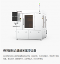
They also have Wafer Chip positioning equipment probably to be paired with their NanoImprint stepper.

They also have Inspection equipment, bonding tools and components like Air flotation platforms.
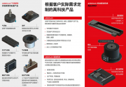
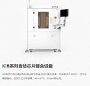

They also have Wafer Chip positioning equipment probably to be paired with their NanoImprint stepper.

They also have Inspection equipment, bonding tools and components like Air flotation platforms.


Star Technology
Guangdong Xingkong Technology Equipment Co., Ltd. (referred to as "Xingkong Technology", English abbreviation "iStar") is headquartered at No. 166 Tashan Avenue, Zengjiang Street, Zengcheng District, Guangzhou.
Smart Starry Sky (Shanghai) Engineering Technology Co., Ltd. is a wholly-owned subsidiary of Starry Sky Technology. It is located in Shanghai and is the product R&D and integration center.
With precision machinery, precision optoelectronics, precision motion, precision control, and complex software as its core technologies, iStar develops innovative equipment in the fields of semiconductors, pan-semiconductors, precision manufacturing, new energy, biomedicine and other fields.
iStar adheres to the mission of "improving the quality of life through innovation" and takes the development of high-end innovative precision intelligent equipment as its own responsibility. It uses "intelligent equipment" to support "Smart China" and "Smart Life", uses technology to change life, and improves people's quality of life. Keep making contributions.
Abstract
| In this paper, we first present a brief review of the advanced-node logic device technology development and its key bottleneck/component processes using the existing lithographic capabilities. It is shown to be feasible to evolve into the GAA era with the minimum change of current FinFET process and a minor refining of previously reported Forksheet structure. The concept of hybrid-channel devices is raised which is not only promising for 3D vertical integration, but also offers an optimal tradeoff between device performance and power/leakage. To address the fabrication challenges, a mandrel/spacer engineering based patterning and metallization technology is proposed and its process development results are reported. This patterning & metallization technique can be applied to fabricate advanced logic and SRAM circuits with significantly enhanced pattern density. It is based on the self-aligned multiple patterning (SAMP) wherein either an alternating arrangement of different materials (with high etching selectivity) or multi-color layer decomposition (i.e., splitting of metallization process) is utilized to solve the edge-placement-error (EPE) issue. In particular, we explore various schemes of self-aligned triple patterning (SATP) to identify the potential solution to ensure a satisfactory profile control of the consecutively formed spacers. Moreover, this technique can incorporate rigorously self-aligned vias & cuts (SAVC), and accommodate a metal-layer division (MLD) to split the neighboring metal lines into two vertically staggered layers with their coupling capacitance significantly reduced. The tested metal Ru allows a direct dry etching, which offers a metal recess capability to enable an alternating-material coverage of neighboring metal wires by two different hard masks such that a selective etching can be applied to form rigorously self-aligned vias. Our early-stage process development is focused on SATP process optimization, fabrication of two simplified grating structures, material screening for appropriate etching selectivity, and metal-layer-division realization. Potential processing challenges such as Ru trench-filling quality and scaling issues of SAVC technology for advanced IC manufacturing will also be discussed. |


