You are using an out of date browser. It may not display this or other websites correctly.
You should upgrade or use an alternative browser.
You should upgrade or use an alternative browser.
Chinese semiconductor thread II
- Thread starter vincent
- Start date
Maskless Lithography machine manufacturer CFMEE.
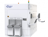
WLP2000 wafer-level advanced packaging direct-write lithography equipment.
Launched two new equipment: a wafer overlay alignment machine and wafer bonding machine. Increasing their footprint in the 2.5D-3D packaging market.

wafer overlay alignment machine.

Wafer bonding Machine

WLP2000 wafer-level advanced packaging direct-write lithography equipment.
Launched two new equipment: a wafer overlay alignment machine and wafer bonding machine. Increasing their footprint in the 2.5D-3D packaging market.

wafer overlay alignment machine.

Wafer bonding Machine
Study of AlN growth using AMEC Prismo HiT3 MOCVD reactor
Advanced Micro-Fabrication Equipment Inc.
Key Laboratory of Advanced Display and System Applications
Abstract
Effect and mechanism of carrier gas velocity, V/III ratio, and carrier gas velocity match of group III to group V (MO VM) on AlN growth rate (GR) were investigated in depth by experiment and computational fluid dynamics (CFD) simulation in Prismo HiT3 MOCVD platform. It is found that AlN growth rate increases with hydrogen flow rate at first, reaches saturation and then shows a monotonic decrease trend. The specific value of turning point depends on the equipment and process. At constant total flow rate of 160 slm, GR increases with MO VM by suppressing parasitic reaction, but uniformity show a deteriorate trend due to the occurrence of turbulence and loss of uniform boundary layer. High quality 4-μm-thick AlN films with improved crystalline quality and atomic smooth surfaces were achieved on nano-patterned sapphire substrates with a growth rate of 0.82 um/hr. The full width at half maximum of the X-ray rocking curve was 162/305 arcsec for (0 0 2)/(1 0 2) planes with total dislocation density ∼ 109 cm−2.

Among the applications of AlN are
- opto-electronics,
- dielectric layers in optical storage media,
- electronic substrates, chip carriers where high thermal conductivity is essential,
- military applications,
- steel and semiconductor manufacturing.
AI Chiplet computing power chip company "Original Chip Semiconductor" completed a new round of financing
AI Chiplet computing power chip company Original Chip (Beijing) Semiconductor Technology Co., Ltd. (hereinafter referred to as Original Chip Semiconductor) recently announced that it has completed a new round of financing . This round of financing was jointly invested by Yiwei Venture Capital, Huafeng Group, etc., and China Science and Technology Innovation Old shareholders such as Xingxing, Zhongguancun Ecological Rainforest Fund, Inno Angel, and Zero2IPO Venture Capital collectively made additional investments . This round of financing will be used for the company's large-model AI Chiplet research and development tape-out and related computing power product development and business expansion.
"Original Semiconductor" is an innovative AI Chiplet computing power chip company, focusing on multi-modal AI processor design technology and Chiplet computing power fusion technology . The company's core team members are all from internationally renowned chip companies and have nearly two decades of industry resources, chip R&D and operation experience. AI chip-related achievements have been acquired by international giants.
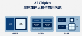
The company can provide one-stop large-model computing power solutions from wafers to accelerator cards/modules, covering customers with diverse needs and various scenarios. The company's products adopt an innovative building block computing power design, and the price/performance ratio is orders of magnitude higher than that of GPUs. Based on the company's innovative AI Chiplet technology and different numbers of chip combinations, the company will launch large model inference accelerator cards and edge large model computing power modules and other cost-effective products with different computing power specifications, while supporting customized computing power.
Semiconductor wafers are important raw materials for manufacturing chips. In the chip lithography process, the surface of the semiconductor wafer is often required to be extremely smooth and flat. However, how to make semiconductors have a mirror-smooth surface has always been one of the key core technologies that restricts the development of my country's chip industry.
Recently, an ultra-precision polishing team from Suzhou University introduced electric fields into the traditional chemical mechanical polishing (CMP) process and developed the first electrochemical mechanical polishing (ECMP) equipment at home and abroad, achieving damage-free, high-precision, and high-efficiency semiconductor polishing. Craftsmanship. Through processing experiments on third-generation semiconductor materials, the surface roughness of semiconductor materials can be reduced to less than 0.22nm, reaching nanoscale processing standards. The efficiency of polishing processing can be increased to 5 times that of existing CMP technology, improving the efficiency of chip companies. Production efficiency is 130%-160%. At the same time, this process can effectively increase the abrasive utilization rate by 32% and significantly reduce the cost of polishing fluid by more than 70%.
Recently, an ultra-precision polishing team from Suzhou University introduced electric fields into the traditional chemical mechanical polishing (CMP) process and developed the first electrochemical mechanical polishing (ECMP) equipment at home and abroad, achieving damage-free, high-precision, and high-efficiency semiconductor polishing. Craftsmanship. Through processing experiments on third-generation semiconductor materials, the surface roughness of semiconductor materials can be reduced to less than 0.22nm, reaching nanoscale processing standards. The efficiency of polishing processing can be increased to 5 times that of existing CMP technology, improving the efficiency of chip companies. Production efficiency is 130%-160%. At the same time, this process can effectively increase the abrasive utilization rate by 32% and significantly reduce the cost of polishing fluid by more than 70%.
It is reported that researchers at the Chinese Academy of Sciences have recently achieved the highest power output of 193 nm and 221 nm lasers using lithium triborate (LBO) crystals. This achievement lays the foundation for more applications of this laser in (DUV) spectrum.
Qinghe Epistar breaks through the preparation of 8-inch SiC bonding substrate
Compared with 6-inch SiC wafers, the available area of 8-inch SiC wafers has almost doubled, and chip output can increase by 80-90%. Upgrading SiC wafers to 8-inches will bring significant benefits to automotive and industrial customers. Therefore, SiC wafers moving towards 8 inches is a recognized development trend in the industry. SiC crystal growth is limited by bottlenecks such as low growth yield and long cycle time, which prevents the cost from being effectively reduced. Advanced SiC bonding substrate technology can bond and integrate high- and low-quality SiC substrates, effectively utilize low-quality crystal growth substrates, and together with the crystal growth technology, significantly reduce the cost of SiC materials, and achieve efficient use of excess traditional productivity. Transformed into new productive forces.
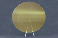
Recently, Qinghe Jingyuan has made important progress in the research and development of SiC bonding substrates through technological innovation. It was the first in China to successfully prepare an 8-inch SiC bonding substrate, further consolidating Qinghe Jingyuan's leadership in this field. status, it is expected to accelerate the mass production of 8-inch SiC substrates and provide more competitive prices for industry customers.
Will be use by SMEE 900A 22nm DUVi?It is reported that researchers at the Chinese Academy of Sciences have recently achieved the highest power output of 193 nm and 221 nm lasers using lithium triborate (LBO) crystals. This achievement lays the foundation for more applications of this laser in (DUV) spectrum.
No output is 1000x too small.Will be use by SMEE 900A 22nm DUVi?

