Chinese semiconductor thread II

tokenanalyst

Brigadier
Registered Member

Weimai Core Materials laid the foundation for 100 tons of high-end semiconductor photolithography materials project​


On March 26, the groundbreaking ceremony of Weimai Core Materials (Hefei) Semiconductor Co., Ltd.'s annual output of 100 tons of semiconductor high-end photolithography materials project was held in Hefei Xinzhan High-tech Zone. After the production is put into operation, localized supply of key photoresist materials will be achieved, and the supply of key photoresist materials will be realized. The stable development of the integrated circuit industry in this area is of great significance.
It is reported that Weimax Core Material (Hefei) Semiconductor Co., Ltd. is a wholly-owned subsidiary of Suzhou Weimax. It is located at the intersection of Yingzhou Road and Longzihu Road in Hefei Xinzhan High-tech Zone, covering an area of 50 acres and with a total investment of 300 million yuan. , aiming to build the largest high-end semiconductor DUV-level (ArF/KrF) photoresist core main material mass production base in China. Products include photoacid generator PAG, BARC layer resin Resin, photoinitiator PI, etc. It also provides intermediates and core monomer materials for each final product. It is planned to build an annual production capacity of 100 tons and will be completed and put into use by the end of the year. .
In recent years, Hefei Xinzhan High-tech Zone has continued to cultivate strategic emerging industries, starting from the "screen" and starting from the "core", gradually forming a "2+5" industrial ecosystem. In the next step, Xinzhan High-tech Zone will strive to become a national high-tech zone, accelerate the construction of a good industrial ecology around the innovation chain, capital chain, talent chain, scenario application, etc., encourage enterprises to further increase R&D investment, and accelerate the iteration of core technologies. Upgrading, accelerating the development of new productive forces, promoting industrial development to a higher level and allowing more flowers to bloom.

Please, Log in or Register to view URLs content!
According to them they already at EUV level so they are one the fews companies offering commercial EUV products.

1711983774909.png
 

antonius123

Junior Member
Registered Member
14 nm is exponentially cheaper than 7 nm just to design, much less fabricate.

Please, Log in or Register to view URLs content!

images-2.png


Agree in term of cost.

But if the performance can surpass NVDIA with 7nm or lower it is amazing.
 

tonyget

Senior Member
Registered Member
Please, Log in or Register to view URLs content!

Exclusive | Tech war: China quietly making progress on new techniques to cut reliance on advanced ASML lithography machines​

Beijing-based Naura Technology Group started research on lithography systems last month, according to people familiar with the matter, as China’s home-grown semiconductor tool makers try workarounds to produce advanced chips without the latest equipment from Dutch giant ASML, a breakthrough that could potentially thwart US attempts to contain China’s chip-making capabilities.

The efforts, which involve multiple players in China’s semiconductor supply chain, have made preliminary research progress, with a patent application by Huawei Technologies last month revealing a technique known as self-aligned quadruple patterning, or SAQP, which can etch lines on silicon wafers multiple times to increase transistor density and chip performance.

The patent, which combines advanced etching and lithography, “will increase the design freedom of circuit patterns”, according to a filing to the China National Intellectual Property Administration, which was first reported by Bloomberg.

By using SAQP with deep ultraviolet lithography (DUV) machines from Dutch giant ASML and Japanese suppliers like Nikon, China could make sophisticated 5-nanometre grade chips without the need for more advanced extreme ultraviolet (EUV) tools only available from ASML.

Chinese companies have been denied access to EUV technology, but have stockpiled DUV machines in recent years amid fears of tighter export controls by Washington and its allies.

Chinese President Xi Jinping told visiting Dutch Prime Minister Mark Rutte in Beijing last week that “no force can stop the pace of China’s scientific and technological development and progress”, while Chinese commerce minister Wang Wentao told his Dutch counterpart Geoffrey van Leeuwen that the Netherlands should fulfil “contractual obligations” and ensure “normal” trade of lithography machines.

Meanwhile, China’s decade-long effort to develop its own lithography machines has hit a wall. The state-owned Shanghai Micro Electronics Equipment Group (SMEE), the country’s sole lithography systems maker, has not come anywhere close to developing machines that match ASML. In December 2022, SMEE was added to a US trade blacklist over national security concerns, meaning it is even less likely to achieve a breakthrough.

A number of Chinese chip tool makers have emerged as important players in efforts to cut the country’s reliance on imported machines. Local semiconductor equipment leader Naura Technology Group has conducted preliminary research into lithography systems since March after it established a special programme last December, according to sources familiar with the matter.

The company has told a small group of engineers to begin research on lithography systems, which is beyond its traditional expertise in etching and film deposition, according to the people, who declined to be named because the discussions were private.

A spokesman for Naura told the Post on Monday the information was not “true”, without elaborating.

While it is far from certain that Naura’s new research efforts will pay off, the move shows the determination by the country’s chip industry to break US-orchestrated sanctions aimed at curbing China’s advances in semiconductors and artificial intelligence.

Meanwhile, these efforts are being conducted in absolute secrecy to avoid further sanctions from Washington, which views them as skirting existing export controls. The US government is considering blacklisting a number of Chinese semiconductor firms linked to Huawei Technologies after the Shenzhen-based tech giant achieved a noticeable breakthrough in advanced chips, Bloomberg reported last month. One of the potential targets is SiCarrier, a state-backed chip tool developer that works with Huawei, and was granted a patent related to SAQP late last year.

The involvement of Chinese firms across the chip tool supply chain is to be expected, as Beijing is pulling resources from all fronts to achieve breakthroughs, analysts said. Dan Hutcheson, vice-chairman of US-based IC research company TechInsights, said China’s SAQP research is likely to involve companies like Naura and SMEE, as etching and deposition expertise was required for lithography.

“It is driven by SiCarrier’s SAQP patent, which replaces optical lithography steps with etch and deposition steps and will help China get to 5-nm,” Hutcheson said.

Shenzhen-based SiCarrier was granted a similar patent by China’s intellectual property authority in December 2023, in which it describes a method to use DUV tools and SAQP to achieve 5-nm node production, according to its filing.

Separately, a research memo by Citigroup analysts claimed that Naura and local rival Advanced Micro-Fabrication Equipment were looking into complementary efforts on a new multiple-patterning technology that uses etching techniques to achieve 7-nm and more advanced chips, according to a Bloomberg report.

To be sure, achieving 7-nm, or even 5-nm grade chips, will still mean China is behind the state of the art. Global foundry leader Taiwan Semiconductor Manufacturing Co produced 3-nm chips for Apple last year, and is scheduled to advance to 2-nm silicon enabled by ASML’s latest EUV machines.

But few are willing to bet against China when Beijing has the ability to mobilise the country’s entire semiconductor supply chain. By the end of 2023, Naura had applied for more than 7,900 patents, and had obtained rights to more than 4,600 of those, according to company stock filing in February.
 

MortyandRick

Senior Member
Registered Member
Please, Log in or Register to view URLs content!

Exclusive | Tech war: China quietly making progress on new techniques to cut reliance on advanced ASML lithography machines​

Beijing-based Naura Technology Group started research on lithography systems last month, according to people familiar with the matter, as China’s home-grown semiconductor tool makers try workarounds to produce advanced chips without the latest equipment from Dutch giant ASML, a breakthrough that could potentially thwart US attempts to contain China’s chip-making capabilities.

The efforts, which involve multiple players in China’s semiconductor supply chain, have made preliminary research progress, with a patent application by Huawei Technologies last month revealing a technique known as self-aligned quadruple patterning, or SAQP, which can etch lines on silicon wafers multiple times to increase transistor density and chip performance.

The patent, which combines advanced etching and lithography, “will increase the design freedom of circuit patterns”, according to a filing to the China National Intellectual Property Administration, which was first reported by Bloomberg.

By using SAQP with deep ultraviolet lithography (DUV) machines from Dutch giant ASML and Japanese suppliers like Nikon, China could make sophisticated 5-nanometre grade chips without the need for more advanced extreme ultraviolet (EUV) tools only available from ASML.

Chinese companies have been denied access to EUV technology, but have stockpiled DUV machines in recent years amid fears of tighter export controls by Washington and its allies.

Chinese President Xi Jinping told visiting Dutch Prime Minister Mark Rutte in Beijing last week that “no force can stop the pace of China’s scientific and technological development and progress”, while Chinese commerce minister Wang Wentao told his Dutch counterpart Geoffrey van Leeuwen that the Netherlands should fulfil “contractual obligations” and ensure “normal” trade of lithography machines.

Meanwhile, China’s decade-long effort to develop its own lithography machines has hit a wall. The state-owned Shanghai Micro Electronics Equipment Group (SMEE), the country’s sole lithography systems maker, has not come anywhere close to developing machines that match ASML. In December 2022, SMEE was added to a US trade blacklist over national security concerns, meaning it is even less likely to achieve a breakthrough.

A number of Chinese chip tool makers have emerged as important players in efforts to cut the country’s reliance on imported machines. Local semiconductor equipment leader Naura Technology Group has conducted preliminary research into lithography systems since March after it established a special programme last December, according to sources familiar with the matter.

The company has told a small group of engineers to begin research on lithography systems, which is beyond its traditional expertise in etching and film deposition, according to the people, who declined to be named because the discussions were private.

A spokesman for Naura told the Post on Monday the information was not “true”, without elaborating.

While it is far from certain that Naura’s new research efforts will pay off, the move shows the determination by the country’s chip industry to break US-orchestrated sanctions aimed at curbing China’s advances in semiconductors and artificial intelligence.

Meanwhile, these efforts are being conducted in absolute secrecy to avoid further sanctions from Washington, which views them as skirting existing export controls. The US government is considering blacklisting a number of Chinese semiconductor firms linked to Huawei Technologies after the Shenzhen-based tech giant achieved a noticeable breakthrough in advanced chips, Bloomberg reported last month. One of the potential targets is SiCarrier, a state-backed chip tool developer that works with Huawei, and was granted a patent related to SAQP late last year.

The involvement of Chinese firms across the chip tool supply chain is to be expected, as Beijing is pulling resources from all fronts to achieve breakthroughs, analysts said. Dan Hutcheson, vice-chairman of US-based IC research company TechInsights, said China’s SAQP research is likely to involve companies like Naura and SMEE, as etching and deposition expertise was required for lithography.

“It is driven by SiCarrier’s SAQP patent, which replaces optical lithography steps with etch and deposition steps and will help China get to 5-nm,” Hutcheson said.

Shenzhen-based SiCarrier was granted a similar patent by China’s intellectual property authority in December 2023, in which it describes a method to use DUV tools and SAQP to achieve 5-nm node production, according to its filing.

Separately, a research memo by Citigroup analysts claimed that Naura and local rival Advanced Micro-Fabrication Equipment were looking into complementary efforts on a new multiple-patterning technology that uses etching techniques to achieve 7-nm and more advanced chips, according to a Bloomberg report.

To be sure, achieving 7-nm, or even 5-nm grade chips, will still mean China is behind the state of the art. Global foundry leader Taiwan Semiconductor Manufacturing Co produced 3-nm chips for Apple last year, and is scheduled to advance to 2-nm silicon enabled by ASML’s latest EUV machines.

But few are willing to bet against China when Beijing has the ability to mobilise the country’s entire semiconductor supply chain. By the end of 2023, Naura had applied for more than 7,900 patents, and had obtained rights to more than 4,600 of those, according to company stock filing in February.
Already posted. Why post again?
I didn't know Naura make lithography?

If China had "hit a wall" in terms of lithography, to then why is it important that Naura is doing it? Will Naura succeed where the whole of china "failed"?
 

tokenanalyst

Brigadier
Registered Member

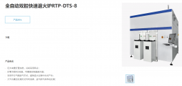
Shengding Precision: Focusing On The Semiconductor Segment, Launching A Fully Automatic Dual-Chamber Rapid Annealing Furnace​


From March 20th to 22nd, the 2024 Munich Shanghai Electronic Production Equipment Exhibition was grandly held at the Shanghai New International Expo Center. During the exhibition, Mr. Ou Jianheng, general manager of the Semiconductor Division of Dongguan Shengding Precision Instrument Co., Ltd., accepted an exclusive media interview with Compound Semiconductor & Semiconductor Core Technology .


Focus on subdivided areas and establish a semiconductor division
According to Ou Jianheng, Dongguan Shengding Precision Instrument Co., Ltd. ("Shengding Precision") was established in 2012. It is a national high-tech enterprise integrating R&D, design, production, sales and industrial chain services. Provide our customers with advanced overall surface treatment and testing solutions in semiconductor, 3C, new energy, display and other fields.
Shengding Precision focuses on equipment development and technology application in the semiconductor field. Currently, it has established a semiconductor business department. Through continuous innovative research and development, it has successfully developed RTP rapid annealing furnace, microwave plasma cleaning machine, PLASMA plasma degumming machine, etc., which are widely used in In the semiconductor industry, it has been recognized by many domestic and foreign mainstream market manufacturers and has achieved a good market reputation.

Core products made a grand appearance, and rapid annealing furnaces attracted much attention

At the Munich Shanghai Electronic Production Equipment Exhibition, Shengding Precision comprehensively displayed equipment and solutions such as RTP rapid annealing furnace, microwave plasma cleaning machine, online vacuum plasma cleaning machine, and atmospheric plasma nano-coating .

1711991395547.png

Ou Jianheng said, "Our fully automatic dual-chamber rapid annealing furnace is the best fully automatic dual-chamber RTP equipment within 5 million in China." It is understood that Shengding Precision fully-automatic dual-chamber rapid annealing furnace has excellent heat source and structural design. It uses double-sided halogen lamp tubes as the heating source, adopts double-sided heating method, and the lamp power PID temperature control can monitor and correct the temperature in real time, achieve precise control of temperature rise, and ensure good reproducibility and temperature uniformity.


Please, Log in or Register to view URLs content!
 

sunnymaxi

Captain
Registered Member
Already posted. Why post again?
I didn't know Naura make lithography?

If China had "hit a wall" in terms of lithography, to then why is it important that Naura is doing it? Will Naura succeed where the whole of china "failed"?
don't take SCMP article serious.. NAURA is not working on Lithography .. its other institutes..

and who told you ?? whole of China failed..

China has successfully completed lithography ecosystem include all core components.. don't you read previous pages of this thread.
 

tokenanalyst

Brigadier
Registered Member
Already posted. Why post again?
I didn't know Naura make lithography?

If China had "hit a wall" in terms of lithography, to then why is it important that Naura is doing it? Will Naura succeed where the whole of china "failed"?
To be honest, etching is absolutely critical in multi-patterning techniques, without a good aspect ratio etching would be impossible to use multi patterning techniques like LEX3 or SAQP, and is one of the reason why the idiots in D.C thought that Huawei was no be able to make 7nm chips even if they have ASML scanners because the necessity of etching machines from LAM and AMAT, so Naura and AMEC upgrading their tools to support the very high aspect ratio structures necessary for multi patterning is as important as SMEE lithography machine.
 

tphuang

Lieutenant General
Staff member
Super Moderator
VIP Professional
Registered Member
The chip gets like 1/3 the performance for 1/10 the cost so you can just stack and scale them.
not so easy unfortunately when it comes to AI, chip-to-chip interconnect speed is an issue. Same with Serdes chips.

Please, Log in or Register to view URLs content!

JLAE has started production of SiC. to be used in electric Drive. Allows for peak 900V platform. Supports 30-80% charging in 7 min.

YASC announces that its new Wuhan production base will be roofed in July and be in production next June. It will produce 30k wpm when fully ramped

JiaSheng semi has been roofed and will started operation in 2025

Lingang is looking to develop 8-inch SiC domestic supply chain with goal of 80k wpm. It has SiCC, Shanghai Jita *& others invested in its area.
 
Top