Chinese semiconductor thread II

paiemon

Junior Member
Registered Member
China a "sustainable 10 year gap" behind in advanced chips according to Intel CEO at Davos. Video in the replies:

Please, Log in or Register to view URLs content!
Let's see how it ages in comparison to other famous Pat Gelsinger comments such as:

"AMD is in the rearview mirror" - accurate considering AMD and Intel are heading in opposite directions based on stock price alone.
"Apple is a lifestyle company" - if the stock price is any indicator, the Apple lifestyle is certainly preferable.
"Nvidia got lucky (in terms of right place, right time for AI)" - Does that mean Pat and his predecessors are back luck charms because Intel has been really unlucky in comparison.

Pat's industry forecasting has been about as reliable as a monkey throwing darts, so we will see how this plays out.
 

tokenanalyst

Brigadier
Registered Member

Research on high-precision EUV reflectance testing technology based on normalization​

1Institute of Microelectronics, Chinese Academy of Sciences
2University of Chinese Academy of Sciences


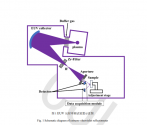
Based on a small reflectivity test device developed using gas discharge plasma (DPP) extreme ultraviolet (EUV) light source, the influence of DPP light source parameters and different types of detectors on reflectivity testing was analyzed, and an energy normalized test device was proposed. Reflectance test method, and tested the reflectance characteristics of Mo/Si multilayer mirror at 13.5nm wavelength. The research results show that under the same light source parameters, the extreme ultraviolet energy detection performance of the SXUV100 detector is better than that of the AXUV100G type; through normalization, the impact factor of light energy fluctuations on the reflectivity test beam is reduced from 6.2% to 0.64%, which is more The measurement repeatability of the peak reflectance of the layer-coated mirror has been increased from 4.34% to 0.69%, which is equivalent to the accuracy of equivalent foreign experimental devices. It has achieved high-precision reflectivity testing and can provide reflectance testing for optical components of extreme ultraviolet lithography machines.​

1705530347294.png


Please, Log in or Register to view URLs content!
 

latenlazy

Brigadier

Research on high-precision EUV reflectance testing technology based on normalization​

1Institute of Microelectronics, Chinese Academy of Sciences
2University of Chinese Academy of Sciences


Based on a small reflectivity test device developed using gas discharge plasma (DPP) extreme ultraviolet (EUV) light source, the influence of DPP light source parameters and different types of detectors on reflectivity testing was analyzed, and an energy normalized test device was proposed. Reflectance test method, and tested the reflectance characteristics of Mo/Si multilayer mirror at 13.5nm wavelength. The research results show that under the same light source parameters, the extreme ultraviolet energy detection performance of the SXUV100 detector is better than that of the AXUV100G type; through normalization, the impact factor of light energy fluctuations on the reflectivity test beam is reduced from 6.2% to 0.64%, which is more The measurement repeatability of the peak reflectance of the layer-coated mirror has been increased from 4.34% to 0.69%, which is equivalent to the accuracy of equivalent foreign experimental devices. It has achieved high-precision reflectivity testing and can provide reflectance testing for optical components of extreme ultraviolet lithography machines.​

View attachment 124061


Please, Log in or Register to view URLs content!
DPP being used as part of the testing equipment supply chain for EUV mirror development is an interesting and cute turn of events lol
 

ZeEa5KPul

Colonel
Registered Member
Let's see how it ages in comparison to other famous Pat Gelsinger comments such as:

"AMD is in the rearview mirror" - accurate considering AMD and Intel are heading in opposite directions based on stock price alone.
"Apple is a lifestyle company" - if the stock price is any indicator, the Apple lifestyle is certainly preferable.
"Nvidia got lucky (in terms of right place, right time for AI)" - Does that mean Pat and his predecessors are back luck charms because Intel has been really unlucky in comparison.

Pat's industry forecasting has been about as reliable as a monkey throwing darts, so we will see how this plays out.
He sounds like the Jim Cramer of semiconductors.
 

tphuang

Lieutenant General
Staff member
Super Moderator
VIP Professional
Registered Member

Xinchi Technology’s automotive chips have shipped more than 3 million pieces in total​

2024 Xinchi Technology New Year Talk" was held in Beijing. Zhang Qiang, chairman of Xinchi Technology, shared the layout and mass production process of Xinchi's "all-scenario intelligent car core" , focusing on the three core application scenarios of smart cabin, smart driving, and smart control, Xinchi has obtained nearly 200 mass production appointments, and its customers cover more than 90% of domestic automotive OEMs, setting a record of cumulative mass production and shipment of more than 3 million pieces. Achievements, covering nearly 40 mainstream models.

Data from the China Association of Automobile Manufacturers shows that the sales volume of self-owned brand passenger cars in 2023 will reach 14.596 million units, an increase of 24.1% from the same period last year, and the market share will rise to 56%, an increase of 6.1 percentage points from the previous year. Xinchi Technology has contributed innovative power to the rapid development of independent brands . According to Xinchi Technology, among the top 15 self-owned brand SUV best-selling cars in 2023, 40% of the models are equipped with Xinchi products; the top 3 in the medium and large SUV field All mass-produced models are equipped with Xinchi cores.

Moreover , the Xinchi X9 cabin series has become the mainstream choice for China's car-grade smart cockpit chips, with dozens of blockbuster designated models. In April 2023, Xinchi released the latest generation smart cockpit chip X9SP, a new member of the X9 series family. As a full-scenario cockpit processor for future mainstream smart cockpit applications, its CPU, GPU and AI computing power have been greatly improved, and it has rich capabilities. Application scenarios enable one chip to cover all functions of future smart cockpits.

Looking forward to 2024, Xinchi will also launch a number of innovative products such as next-generation integrated cabin and driver chips and next-generation high-performance MCUs for regional controllers.

Please, Log in or Register to view URLs content!
their English name is SemiDrive.

Yes, they are a big deal. and the goal of 20% market share by 2025 is quite impressive.

Please, Log in or Register to view URLs content!

I've talked about them quite a bit in the past, but the increased sales should allow them to fab cockpit chips at more advanced foundries and use A78AE cores
 

tokenanalyst

Brigadier
Registered Member

With a total investment of 500 million yuan, Jiangsu has added a new semiconductor grade material project​

Shanghai Xijia Precision Company and Jiangsu Meilan Group held a signing ceremony at the Taixing Economic Development Zone Management Committee for the Jiangsu Ximei semiconductor grade material project . The total planned investment of the project is 500 million yuan, with a land area of 30 acres. After completion, the annual output value will reach 1.5 billion yuan. The implementation of this project will effectively break the foreign monopoly on FFKM and PFA.

Perfluoroether rubber (FFKM) and fusible fluororesin (PFA) for the semiconductor industry are mainly used in the semiconductor industry, human medicine and aerospace fields.

It is reported that Shanghai Xijia Precision Company is a manufacturer of polymer elastomers and high-functional plastic sealing products. This cooperation with Meilan aims to share resources and achieve a win-win situation. The success of the signing between the two parties is the starting point for the cooperation between the two parties.

Please, Log in or Register to view URLs content!
 

siegecrossbow

General
Staff member
Super Moderator
Please, Log in or Register to view URLs content!

Talent pool to draw from for semiconductor factory technicians in the US are fastfood workers.

If they do massive tech layoffs this year I’ve got a backup plan. I may not be top notch but at least I’ve got legit clean room experience a decade ago, an EE degree from a highly ranked Engineering school, and operational experience of expensive equipment like electron microscopes. All of which beats burger flipping in my humble opinion.
 

tokenanalyst

Brigadier
Registered Member

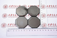
Professor Wang Hongxing’s team at Xi’an Jiaotong University achieved mass production of 2-inch heteroepitaxial single crystal diamond substrates​


A research team from Xi'an Jiaotong University used microwave plasma chemical vapor deposition (MPCVD) technology to successfully mass-produce 2-inch heteroepitaxial single-crystal diamond self-supporting substrates.

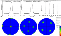
The team improved the yield of heteroepitaxial single crystal diamond by effectively controlling the film formation uniformity, temperature field and flow field. The substrate surface has a step-flow growth mode, which can reduce the defect density of the substrate and improve the crystal quality. The half-peak widths of XRD (004) and (311) rocking curves are less than 91arcsec and 111arcsec respectively, reaching the world's leading level.

1705577942499.png

Diamond semiconductors have material properties such as ultra-wide bandgap, high breakdown field strength, high carrier saturation drift velocity, high thermal conductivity, and excellent device quality factors. Diamond substrates can be used to develop high-temperature, high-frequency, high-power, Radiation-resistant electronic devices overcome technical bottlenecks such as "self-heating effect" and "avalanche breakdown" of devices, and play an important role in the development of 5G/6G communications, microwave/millimeter wave integrated circuits, detection and sensing and other fields. Currently, the development of diamond electronic devices is limited by large-size, high-quality single crystal substrates. The commercialization of silicon, sapphire and other substrates has provided prerequisites for heteroepitaxial single crystal diamond.

1705577982231.png

It is reported that the Wide Bandgap Semiconductor Materials and Devices Research Center of Xi'an Jiaotong University was established in 2013. The director of the laboratory is Professor Wang Hongxing, a nationally appointed expert. After nearly 10 years of development, the laboratory has formed a series of technologies such as diamond semiconductor epitaxial equipment research and development, single crystal/polycrystalline substrate growth, and electronic device development with independent intellectual property rights, and has been authorized 48 patents.

According to Shaanxi Venture Capital, in order to accelerate the rapid industrialization of this technology, Professor Wang Hongxing led the team to establish Xi'an Demonte Semiconductor Technology Co., Ltd. in 2016, and fully launched the transformation and application of relevant technological achievements in the market. In 2021, Shaanxi Venture Capital Hanzhong Fund invested 15 million yuan in Demont Semiconductor to assist Demont Semiconductor in establishing its R&D and production base in Hanzhong High-tech Zone. Demont Semiconductor has built a pilot production line in Hanzhong.


Please, Log in or Register to view URLs content!
 

tphuang

Lieutenant General
Staff member
Super Moderator
VIP Professional
Registered Member

Professor Wang Hongxing’s team at Xi’an Jiaotong University achieved mass production of 2-inch heteroepitaxial single crystal diamond substrates​


A research team from Xi'an Jiaotong University used microwave plasma chemical vapor deposition (MPCVD) technology to successfully mass-produce 2-inch heteroepitaxial single-crystal diamond self-supporting substrates.

The team improved the yield of heteroepitaxial single crystal diamond by effectively controlling the film formation uniformity, temperature field and flow field. The substrate surface has a step-flow growth mode, which can reduce the defect density of the substrate and improve the crystal quality. The half-peak widths of XRD (004) and (311) rocking curves are less than 91arcsec and 111arcsec respectively, reaching the world's leading level.

View attachment 124083

Diamond semiconductors have material properties such as ultra-wide bandgap, high breakdown field strength, high carrier saturation drift velocity, high thermal conductivity, and excellent device quality factors. Diamond substrates can be used to develop high-temperature, high-frequency, high-power, Radiation-resistant electronic devices overcome technical bottlenecks such as "self-heating effect" and "avalanche breakdown" of devices, and play an important role in the development of 5G/6G communications, microwave/millimeter wave integrated circuits, detection and sensing and other fields. Currently, the development of diamond electronic devices is limited by large-size, high-quality single crystal substrates. The commercialization of silicon, sapphire and other substrates has provided prerequisites for heteroepitaxial single crystal diamond.

View attachment 124084

It is reported that the Wide Bandgap Semiconductor Materials and Devices Research Center of Xi'an Jiaotong University was established in 2013. The director of the laboratory is Professor Wang Hongxing, a nationally appointed expert. After nearly 10 years of development, the laboratory has formed a series of technologies such as diamond semiconductor epitaxial equipment research and development, single crystal/polycrystalline substrate growth, and electronic device development with independent intellectual property rights, and has been authorized 48 patents.

According to Shaanxi Venture Capital, in order to accelerate the rapid industrialization of this technology, Professor Wang Hongxing led the team to establish Xi'an Demonte Semiconductor Technology Co., Ltd. in 2016, and fully launched the transformation and application of relevant technological achievements in the market. In 2021, Shaanxi Venture Capital Hanzhong Fund invested 15 million yuan in Demont Semiconductor to assist Demont Semiconductor in establishing its R&D and production base in Hanzhong High-tech Zone. Demont Semiconductor has built a pilot production line in Hanzhong.


Please, Log in or Register to view URLs content!
this is pretty huge. I think it has already been achieved outside of China
Please, Log in or Register to view URLs content!


you need at least 2-inch to be viable for semiconductor industry. This opens up the door for various GaN-on-Diamond products like RF modules, tht will be so important in the future.

Looks like they also used MPCVD here

DiamondGaNResearch_CETC46thInstitute_Dec2023.png
here is demonstration of GaN-on-diamond and its performance vs even GaN-on-Sic substrate
 
Last edited:
Top