
You are using an out of date browser. It may not display this or other websites correctly.
You should upgrade or use an alternative browser.
You should upgrade or use an alternative browser.
Chinese semiconductor thread II
- Thread starter vincent
- Start date
U-Precision delivering its W2W Fusion Bonding Equipment to customer. Another milestone for the company after its D2W chiplet hybrid bonding equipment got delivered in 2026/2/4
This equipment/technology can be used for 3D IC stacking. It fills a whole in China's advanced packaging equipment, especially HBM supply chain, where domestic market share is 5%.
Can be used to vertically stack multiple DRAM chip layers
Uprecision, Piotech, ISabers look like they are big three in bonding technology in China. Piotech and ISabers looks like they have a more complete with metrology and surface treatment. U-precision seems to be weaker in that part but given that they do wafers stages for lithography machines, I estimate that their tools are the most precise in the market, thought HB precision is in the range of 200nm to a few microns.
U-Precision delivering its W2W Fusion Bonding Equipment to customer. Another milestone for the company after its D2W chiplet hybrid bonding equipment got delivered in 2026/2/4
This equipment/technology can be used for 3D IC stacking. It fills a whole in China's advanced packaging equipment, especially HBM supply chain, where domestic market share is 5%.
Can be used to vertically stack multiple DRAM chip layers


UAI Intelligent Technology transforms mobile operation robots into "intelligent nodes" on semiconductor production lines.
UAI Intelligent Technology is transforming mobile operation robots into "intelligent nodes" for semiconductor manufacturing through its "One Brain, Multiple States" embodied intelligence system.
UAI Intelligent Technology continues to make breakthroughs. The OW12-300 and OW8-350 robots can achieve an empty-to-full exchange time of up to 25 seconds , equivalent to the OHT level. They can operate continuously 24/7 , ensuring the production line operates efficiently around the clock.

- Precision & Reliability: ±2mm positioning accuracy, 0.1g vibration control, ISO Class 3 cleanroom compliance, and 360° safety sensors enable continuous 24/7 operation with OHT-level exchange speeds (as fast as 25 seconds).
- Smart Cluster Scheduling: Real-time perception of road conditions, equipment load, and order flow allows dynamic task allocation and global traffic optimization, supporting thousands of heterogeneous robots working in unison.
- Full Closed-Loop Integration: Seamlessly connects with WMS/MES systems and factory infrastructure (elevators, auto-doors) to provide visualized tracking, end-to-end traceability, and safe material handling.
- Comprehensive Coverage: Deploys across the entire semiconductor chain—from upstream wafers/substrates to downstream packaging/testing—and adapts to unstructured Sub-Fab environments via the flexible "Tianyan" series robots.
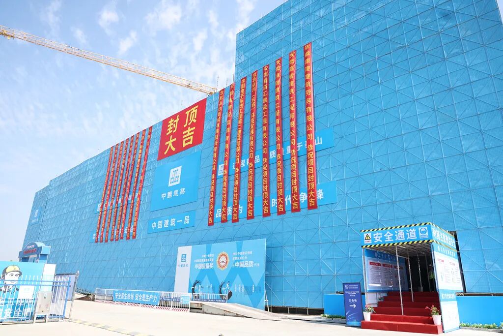
A multi-billion yuan project in Hefei! The main structure of the Jingmei Semiconductor high-end photomask project has been completed.
According to a news release from Hefei High-tech Zone, the main structure of the Jingmei Semiconductor high-end photomask project was recently completed, three weeks ahead of schedule. The first phase of the project involves an investment of 6.5 billion yuan, with a total construction area of 46,000 square meters, focusing on the research, development, production, and sales of 28nm and above high-end photomasks. The project plans to build a high-standard automated production line with a monthly capacity of 3,200 wafers after full production. It is expected to officially start production in 2027, at which time it will become an important high-end photomask production base in China.
On the morning of October 25, 2025, the Anhui Magnesium Photomask Project, with a total investment of 12 billion yuan, officially commenced construction in Hefei High-tech Zone, marking a significant step forward in China's independent and controllable capabilities in the field of high-end photomasks.
Photomasks, hailed as the "mother of chips," are a core component of semiconductor manufacturing. As an independent third-party manufacturer of high-end semiconductor photomasks, Crystal Magnesium Photomasks leverages its advanced technology and flexible service models to precisely meet the needs of domestic and international chip design and wafer manufacturing companies, effectively alleviating reliance on imported high-end photomasks and contributing to the industry's self-reliance and control. Hefei High-tech Zone announced that the successful completion of the project's main structure marks a crucial step forward in the "High-tech Manufacturing" of high-end photomasks. Once completed and put into operation, it will fill a key gap in the regional integrated circuit industry chain, contributing to the industry's steady development.
Oriental Crystal Technology showcased its electron beam quantity measurement technology for advanced process technologies at the 7th China Laboratory Development Conference.
At the recent 7th China Laboratory Development Conference (CLC2026) held in Beijing, Oriental Crystal Technology made significant strides by showcasing its advanced electron beam quantity measurement technology within the broader context of laboratory ecosystem innovation. The conference, themed around foresight, integration, and innovation, gathered industry leaders to discuss new pathways for technological advancement. During the Semiconductor Instrumentation Technology session, Dr. Sun Weiqiang, Vice President of Oriental Crystal Source (DJEL), delivered a keynote speech titled "Electron Beam Metrology Technology for Advanced Process Manufacturing." This presentation systematically outlined the critical role of electron beam metrology in advanced integrated circuit processes, highlighting both the company's localization efforts and its strategic roadmap for future development.
High-end metrology equipment serves as the essential "ruler" and "eye" for chip manufacturing, playing a pivotal role in controlling yields, optimizing iterations, and detecting minute defects across all stages of production. However, these instruments have historically been a major bottleneck restricting China's breakthroughs in advanced semiconductor processes due to long-standing overseas monopolies. To address this challenge, DJEL® has adhered strictly to its commitment for independent research and self-reliance, leveraging its independently controllable Electron Optical System (EOS). This foundational technology has enabled the company to develop a comprehensive SEpA® series of electron beam metrology equipment including EBI, CD-SEM, DR-SEM, and HV-SEM filling critical gaps in the domestic high-end inspection market.

In his address, Dr. Sun tackled three core technical challenges that define modern industry standards: imaging accuracy, mass production capacity, and intelligent algorithms. Regarding accuracy, DJEL utilizes advanced optics like immersion composite mirrors and spherical aberration correction to push spatial resolution limits, while employing 40-60kV high-energy electron beams for deep structural inspections essential in complex multi-layer processes. To enhance capacity, the company overcame bottlenecks in positioning and signal compensation by introducing multi-electron beam imaging technology; this parallel processing approach replaces slow single-point scanning with high-speed online inspection, significantly boosting productivity to meet the rigorous demands of wafer fabrication lines.
Furthermore, DJEL has revolutionized the industry through its self-developed intelligent algorithm system, which integrates AI capabilities into every stage of measurement and inspection. By combining automatic defect classification, image enhancement, recipe generation, and automated equipment adjustment with their PanGen Sim® simulation tools, the company has shifted from passive problem detection to a proactive "design-simulation-prediction-measurement" ecosystem. These innovations are driving continuous process iterations and yield improvements. Looking ahead, Oriental Crystal remains dedicated to independent innovation, aiming to further break through industry barriers with core products that will empower China's chip manufacturing sector toward full technological autonomy and international competitiveness.
Pengkan Semiconductor completes over 100 million RMB Series B financing.
In May 2026, Pengkan Integrated Circuit (Hangzhou) Co., Ltd. (hereinafter referred to as "Pengkan Semiconductor") officially announced the completion of a Series B financing round exceeding RMB 100 million. This round of financing was jointly led by Yangtze Optical Fibre and Cable Industry Fund, Jiangsu Yunrongtong, and CAS Star, with follow-on investments from multiple industrial capital and professional funds, including Fujian Electronics Investment, Hangzhou Data Group, and Anfeng Venture Capital. The scale and lineup of financing fully validate Pengkan's core value and industrial position in the fields of optical communication chips, Physical AI, fiber optic on-board systems, and AIDC infrastructure.
This round of funding will focus on the on-vehicle verification, automotive-grade certification, and mass production of the world's first automotive TS-PON® chip. Simultaneously, it will accelerate the R&D and application expansion of next-generation products such as AIDC optoelectronic interconnect, embedded intelligent optical neural networks, and Industry 4.0 optical networks, supporting the company's comprehensive transition from technology verification to a new stage of large-scale commercialization.


As a pioneer in deterministic optical network communication and a provider of optical interconnect foundations for Physical AI, Pengkan Semiconductor has long focused on high-bandwidth, ultra-low latency, and high-reliability optical communication chips and system solutions. Its independently developed TS PON® technology boasts three core advantages: microsecond-level latency, nanosecond-level full-network synchronization, and single-fiber bidirectional 10G/25G ultra-high bandwidth. It fundamentally solves the key pain points of traditional copper cables and Ethernet in edge AI, intelligent agents, and autonomous driving scenarios—namely, insufficient bandwidth, latency jitter, complex cabling, and poor anti-interference making it a core foundation for the next generation of "optical neural networks" for the Physical AI era. Pengkan also provides low-latency, high-reliability, and easily scalable interconnect solutions for AI data centers (AIDCs) and edge computing clusters.