Chinese semiconductor thread II

interestedseal

Junior Member
Registered Member
At this week's Semicon China expo in Shanghai, state-owned Naura Technology Group, China's largest chip equipment maker, touts in a video that its machines can handle the 7-nanometer production process that makes chips used in smartphones.

Please, Log in or Register to view URLs content!

A brief summary of Semicon China 2024. The expo looked very crowded, and sentiments optimistic.
 

PopularScience

Junior Member
Registered Member
To the experts what is a "brute force" method? And if effective why don't other leading FAB producer used this method?

Please, Log in or Register to view URLs content!

Please, Log in or Register to view URLs content!

Please, Log in or Register to view URLs content!

Please, Log in or Register to view URLs content!


57 minutes ago — Huawei Technologies Co. and a secretive chipmaking partner in China have filed patents for a low-tech but potentially effective way to make ...
6EC8E84A-085B-4EEA-9247-7D4DCA0F85A9.jpegED1BFFFD-81B4-4620-86D7-A5D5C983628E.jpeg
 

olalavn

Senior Member
Registered Member
Recently, Gaoche Technology Co., Ltd. signed a new order for its 8-inch semiconductor diamond wire slicer. After the equipment is delivered, it will be shipped to a European semiconductor company. This is the first overseas customer for the company's semiconductor equipment.
Please, Log in or Register to view URLs content!
 

measuredingabens

Junior Member
Registered Member
what other things required for CEFT process. by 2026 EUV prototype will be in full scale testing .. you meant there is not enough R&D for CFET process yet ? i think we have seen some Chinese institutes exploring this tech ..
It's more that SMIC + Huawei are aiming to commercialise CFETs ~5 years ahead of other foundries. A look at TSMC's roadmap puts their CFET introduction at at 2030+.
Well, in fairness he was very confident about EUV, but only said CFET is likely by 2026.

What I'm more surprised about is his claim that Huawei Ascend 920 is going to be H100 levels as well as to be made on N+2 and not N+3. Kind of strange that they can get that performance without going to 5nm.
Outside of the process advancements, Huawei also has a lot of time to experiment with chip design. The performance difference between the H100 and Nvidia's upcoming products is very large and yet they are still using TSMC's customised N4 out to their GB200.
 
Last edited:

sunnymaxi

Major
Registered Member
It's more that SMIC + Huawei are aiming to commercialise CFETs ~5 years ahead of other foundries. A look at TSMC's roadmap puts their CFET introduction at at 2030+.
hmm.. once SMIC/Huawei get their hands on EUV. it will be relatively easy for them to experiment.. Chinese institutes exploring different architecture for advanced nodes as we have seen research papers.. Huawei also doing own research in advanced nodes..
 

latenlazy

Brigadier
that actually is quite plausible based on what we've seen. Both @latenlazy and I think they will have prototype unit at SMIC next year to start test and validation of EUV process. I'm more unconvinced of his claim of CFET. That seems really far fetched
what other things required for CEFT process. by 2026 EUV prototype will be in full scale testing .. you meant there is not enough R&D for CFET process yet ? i think we have seen some Chinese institutes exploring this tech ..
Well, in fairness he was very confident about EUV, but only said CFET is likely by 2026.

What I'm more surprised about is his claim that Huawei Ascend 920 is going to be H100 levels as well as to be made on N+2 and not N+3. Kind of strange that they can get that performance without going to 5nm.
IMG_1101.jpegIMG_1102.jpeg

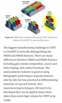
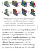
I think CFET is plausible because you can research different fabrication techniques in parallel and there’s no reason not to while you are bottlenecked elsewhere. Vertical stacking seems to require some new techniques that may not leverage continuing competences from GAAFET so it makes sense to explore. Nothing dictates that you need to deploy the new architecture at a sub 3 nm node like Samsung or TSMC since you don’t have a guaranteed production pipeline to manage schedule risk around anyways.


hmm.. once SMIC/Huawei get their hands on EUV. it will be relatively easy for them to experiment.. Chinese institutes exploring different architecture for advanced nodes as we have seen research papers.. Huawei also doing own research in advanced nodes..
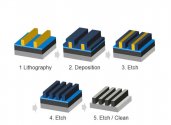
Etching and deposition techniques and their quality are the primary innovation pressure points for new architectures. Lithography resolution primarily pushes feature size innovation (a bit of a simplification since detail sharpness does matter but in this case a useful one to understand what research enablers and constraints are).
 

sunnymaxi

Major
Registered Member
Etching and deposition techniques and their quality are the primary innovation pressure points for new architectures. Lithography resolution primarily pushes feature size innovation (a bit of a simplification since detail sharpness does matter but in this case a useful one to understand what research enablers and constraints are).
thanks a lot.. you have cleared many critical points

NAURA is front runner in Etching technology.. remember @tokenanalyst posted this news.
---------------------------------------------------------------------------------------------------------
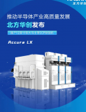
Beast of a Etching machine developed by NAURA..
1710545071252.png

As a key technical equipment in the semiconductor manufacturing industry chain, the development level of etching machines directly affects the miniaturization, performance improvement and yield control of integrated circuits. It is the core driving force for the high-quality development of the semiconductor industry. With the expansion of domestic logic chip production capacity, the industry's demand for 12-inch key process dielectric etching machines has increased. At the same time, the continuous advancement of domestic memory chip technology and the continued expansion of production capacity will also drive a considerable number of CMOS key process dielectric etching machines.

  In order to promote the high-quality development of the semiconductor industry, Northern Huachuang has established a professional R&D team to develop Accura LX, a 12-inch dielectric etching machine for key processes. Its process performance has exceeded the current industry indicators: through Continue plasma (continuous plasma) settings and Optimization of the transmission process can achieve higher productivity while ensuring product yield; through the high-density opening rate design of the Shower head (gas inlet silicon electrode), excellent product uniformity can be achieved and equipment Fatal arcing can be reduced. ) risk; in addition, the machine is equipped with various forms of radio frequency pulse functions to achieve a high selection ratio of Mask and Stop layer, and reduce device damage; the multi-zone air source flow control and The temperature adjustment design can achieve precise adjustment in micro areas to meet customer customized needs. The excellent performance of Accura LX equipment has been favored by many customers, and a number of process verifications have been completed.

  Accura LX equipment, as a 12-inch dual Damascus CCP (capacitively coupled plasma) dielectric etching product launched by Northern Huachuang, has opened up a new product market field for Northern Huachuang and can be compared with the existing 12-inch silicon and metal etching products. The machine forms a complete etching process solution. At the same time, the 12-inch CCP etching machine hardware architecture and technology platform built by Accura LX can be used in storage, CIS (complementary metal oxide semiconductor image sensor), Power (power semiconductor) and other fields, and has broad application prospects.

  In the future, Northern Huachuang will rely on its profound technology accumulation and R&D capabilities to continue to delve into the equipment market in the field of dielectric etching, continue to innovate and optimize the performance of dielectric etching equipment, promote the accuracy, yield and production capacity of integrated circuit manufacturing, and then meet the new requirements. The urgent demand for high-performance chips in a generation of information technology products drives industrial progress and creates unlimited possibilities.
----------------------------------------------------------------------------------------------
Chinese equipment companies progressing very fast in Non-Litho tools.. so once SMIC get EUV prototype and along with these Etching machine. so CFET fabrication process is very much plausible in 2026-27 ? right
 
Top