Chinese semiconductor thread II

tokenanalyst

Brigadier
Registered Member
Ehh this is a milliwatt laser though so almost definitely not for lithography.
To be clear. All RSLaser DUV light source that are going to be mass produced and delivered (60W 6KHZ 193nm and 40W 4KHZ 248nm) for now are going ArF and KrF gas excimer powered lasers.

But definitely I think solid states DUV lasers are going to replace excimer gases powered light sources. In the same way that I think FEL EUV are going to replace plasma produced light sources.

Gigaphoton Hybrid solid state 193nm DUV laser:
Please, Log in or Register to view URLs content!
 

Phead128

Captain
Staff member
Moderator - World Affairs
I'll say Bring it on, it will be a badge of honor to be included with the likes of Huawei and other sanction company with a free advert to booth. ;)

Please, Log in or Register to view URLs content!

Please, Log in or Register to view URLs content!

Please, Log in or Register to view URLs content!

Please, Log in or Register to view URLs content!


43 minutes ago — The Biden administration is considering blacklisting a number of Chinese semiconductor firms linked to Huawei Technologies after the telecom ...
Is this the 274th attempt to definitely and absolutely destroy Huawei? At this point, they are milking this for the electoral value or virtue signalling. These additional sanctions make no difference.
 

measuredingabens

Junior Member
Registered Member
Please, Log in or Register to view URLs content!

High performance artificial visual perception and recognition with a plasmon-enhanced 2D material neural network

Abstract

The development of neuromorphic visual systems has recently gained momentum due to their potential in areas such as autonomous vehicles and robotics. However, current machine visual systems based on silicon technology usually contain photosensor arrays, format conversion, memory and processing modules. As a result, the redundant data shuttling between each unit, resulting in large latency and high-power consumption, seriously limits the performance of neuromorphic vision chips. Here, we demonstrate an artificial neural network (ANN) architecture based on an integrated 2D MoS2/Ag nanograting phototransistor array, which can simultaneously sense, pre-process and recognize optical images without latency. The pre-processing function of the device under photoelectric synergy ensures considerable improvement of efficiency and accuracy of subsequent image recognition. The comprehensive performance of the proof-of-concept device demonstrates great potential for machine vision applications in terms of large dynamic range (180 dB), high speed (500 ns) and low energy consumption per spike (2.4 × 10−17 J).
 

measuredingabens

Junior Member
Registered Member
Please, Log in or Register to view URLs content!

Biomimetic nanocluster photoreceptors for adaptative circular polarization vision

Abstract

Nanoclusters with atomically precise structures and discrete energy levels are considered as nanoscale semiconductors for artificial intelligence. However, nanocluster electronic engineering and optoelectronic behavior have remained obscure and unexplored. Hence, we create nanocluster photoreceptors inspired by mantis shrimp visual systems to satisfy the needs of compact but multi-task vision hardware and explore the photo-induced electronic transport. Wafer-scale arrayed photoreceptors are constructed by a nanocluster-conjugated molecule heterostructure. Nanoclusters perform as an in-sensor charge reservoir to tune the conductance levels of artificial photoreceptors by a light valve mechanism. A ligand-assisted charge transfer process takes place at nanocluster interface and it features an integration of spectral-dependent visual adaptation and circular polarization recognition. This approach is further employed for developing concisely structured, multi-task, and compact artificial visual systems and provides valuable guidelines for nanocluster neuromorphic devices.
 

tokenanalyst

Brigadier
Registered Member

Xinyuan Micro's (KingSemi) Shanghai Lingang factory was officially completed and put into production​


It is reported that Shanghai Xinyuan Micro Synchronous released the first self-developed high-end equipment-KCE front-end single-chip chemical cleaning machine. This model has the advantages of high process coverage, high stability, high cleanliness, high productivity, and high intelligence. It has a self-developed 16 champer high-capacity architecture, the process coverage can reach more than 80%, and it is suitable for high-temperature SPM processes. . Currently, Wafer Demo testing has been carried out for nearly ten customers, and many process levels have reached industry-leading levels.

1711025251750.png

Please, Log in or Register to view URLs content!
 

tokenanalyst

Brigadier
Registered Member

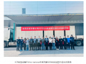
The 500th unit of the Primo nanova® series of ICP etching equipment from AMEC is shipped​

China Microelectronics Corporation announced that the 500th reaction chamber of the company's Primo nanova® series of inductively coupled plasma (ICP) etching equipment was successfully shipped to an advanced domestic semiconductor chip manufacturer recently. The ICP etching equipment Primo nanova® series products shipped in this batch are all from repeat orders from this customer.
1711030465130.png
The Primo nanova® shipped this time is a 12-inch etching equipment developed by AMEC based on inductive coupling (ICP) technology for various key applications in advanced process nodes and production lines. It is suitable for advanced logic chips and DRAM memory chips. and etching of 3D NAND memory chips.

1711030548339.png

The plasma etching equipment and chemical thin film equipment developed by China Microelectronics Corporation are key equipment for manufacturing various micro-devices, and can process various devices at the micron and nanoscale. It is reported that AMEC's plasma etching equipment has been widely used in many etching applications in advanced processes of international front-line customers. The MOCVD equipment developed by AMEC for the production of LED and power device epitaxial wafers has been put into use in customer production lines. production, currently occupying a dominant position in the global gallium nitride-based LED MOCVD equipment market.
In addition, data show that in 2023, China Micro's operating income will be approximately 6.264 billion yuan, an increase of approximately 1.524 billion yuan compared with 2022, a year-on-year increase of approximately 32.15%. Among them, etching equipment revenue in 2023 will be approximately 4.703 billion yuan, a year-on-year increase of approximately 49.43%. Etching equipment, which accounts for approximately 75.1% of the company's operating revenue, will grow by 55.4% and 57.1% in 2021 and 2022, respectively. The total value of new orders from China Microsystems in 2023 will be approximately 8.36 billion yuan, an increase of approximately 2.04 billion yuan from 2022, a year-on-year increase of 32.3%, of which new orders for etching equipment will reach 6.95 billion yuan, a year-on-year increase of approximately 60.1%.

Please, Log in or Register to view URLs content!
 

tokenanalyst

Brigadier
Registered Member

Northern Huachuang's high dielectric constant atomic layer deposition equipment received batch orders​


On March 21, Northern Huachuang announced that the company's 12-inch high dielectric constant atomic layer deposition equipment Scaler HK430 has recently achieved stable mass production and received batch orders. This marks the successful application of Northern Huachuang's CVD (Chemical Vapor Deposition) advanced process equipment solution.

In order to break through the process bottleneck of transistor size shrinkage, the industry uses the new High-K material HfO 2 (hafnium oxide) as the gate dielectric layer, combined with metal gate technology, to develop HKMG (High-K/Metal Gate high dielectric constant/metal gate). Extremely) craftsmanship.

Northern Huachuang said that this process occupies a core position at 45nm and below nodes, and CVD/ALD (atomic layer deposition) process equipment has become an important support for the HKMG process.

Please, Log in or Register to view URLs content!
 

tokenanalyst

Brigadier
Registered Member

New progress has been made in the heterogeneous integration of thick-film gallium nitride and polycrystalline diamond in microelectronics​


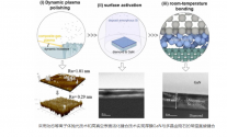
Recently, the team of researcher Liu Xinyu from the High Frequency and High Voltage Center of the Institute of Microelectronics, in cooperation with Tianjin Zhongke Jinghe Company and other units, has made new progress in the field of direct bonding technology between thick film gallium nitride (GaN) and polycrystalline diamond. This study uses dynamic plasma polishing (DPP) technology to reduce the convex peak height on the polycrystalline diamond surface from 15nm to 1.2nm, obtaining a smooth surface with a surface roughness of 0.29nm, and combines it with the surface activation bonding method at room temperature. Achieved direct bonding of ~370μm GaN and ~660μm polycrystalline diamond substrate, with a bonding rate of ~92.4% and can withstand ambient temperatures of -55℃~250℃, providing an effective solution for wafer-level polycrystalline diamond bonding technical approach.

In recent years, the GaN/diamond heterogeneous integration method has become one of the effective ways to achieve high reliability and high power density GaN-based high electron mobility transistors (HEMTs). Direct wafer bonding technology has the advantages of high interface thermal conductivity and low thermal stress, and is promising in the integration of materials and devices, but it has high quality requirements such as material surface profile and roughness. At present, single crystal diamond can barely obtain the low surface roughness and high flatness required for direct bonding through chemical mechanical polishing technology (CMP), and small-size direct bonding can be achieved in the early stage. However, the large-size growth problem of single crystal diamond greatly limits its application, and the cost remains high. Polycrystalline diamond has the advantages of low cost and large size, but it has many problems such as many grain boundaries, uneven stress, irregular pits and ridges, etc., making it difficult for CMP technology to meet the requirements of surface roughness and surface flatness at the same time. and other requirements, it is difficult to achieve direct bonding. On the other hand, thick-film GaN can be combined with technologies such as Smart-Cut® to achieve compound semiconductor manufacturing and heterostructure construction, but thick-film GaN bonds also face greater stress issues. Currently, there are very few studies on the direct bonding of thick-film GaN and polycrystalline diamond.
1711031386793.png

This study uses plasma polishing technology with dynamic incident angles to solve surface morphology problems such as polycrystalline diamond flatness and roughness in a pressure-free state, combined with an ion beam surface activation bonding method assisted by in-situ silicon nanolayer deposition. The heterogeneous integration of thick film GaN and polycrystalline diamond was achieved, with a bonding rate of ~92.4%. The team used variable temperature confocal Raman spectroscopy technology to study the residual stress of the GaN/diamond bonding interface in the temperature range of -55°C to 250°C and its changes with temperature. They found that the GaN/diamond bonding interface at room temperature has ~200 MPa residual stress, and the interface stress increases asymmetrically when the temperature increases, that is, the stress on the diamond side increases significantly, while the stress on the GaN side does not change much. This is attributed to the fact that GaN and silicon nanobonding auxiliary layers have similar coefficients of thermal expansion (CTE), while the CTEs of diamond and silicon nanobonding auxiliary layers are quite different. This asymmetric interfacial stress demonstrates the effectiveness of the amorphous silicon nanolayer as a buffer layer to relieve stress.


Please, Log in or Register to view URLs content!
 

siegecrossbow

General
Staff member
Super Moderator
I'll say Bring it on, it will be a badge of honor to be included with the likes of Huawei and other sanction company with a free advert to booth. ;)


Please, Log in or Register to view URLs content!

Please, Log in or Register to view URLs content!

Please, Log in or Register to view URLs content!

Please, Log in or Register to view URLs content!


43 minutes ago — The Biden administration is considering blacklisting a number of Chinese semiconductor firms linked to Huawei Technologies after the telecom ...

1711031767873.jpeg
What didn’t work between 2018 and 2023 will definitely work in 2024.
 
Top