At this point if you're a semiconductor company in China and not sanctioned, it means either you have yet to join the big boys or you have no chance of joining them as Uncle Sam deems.
You are using an out of date browser. It may not display this or other websites correctly.
You should upgrade or use an alternative browser.
You should upgrade or use an alternative browser.
Chinese semiconductor thread II
- Thread starter vincent
- Start date
The gall of this guy, Of course you can, with a big help from Uncle Sam and from harvested TSMC.
Intel CEO: 'Our goal is to have at least 50% of the world's advanced semiconductors produced in the U.S. and Europe by the end of the decade' Pat Gelsinger is the CEO of Intel Corporation. Chips are the sinews and synapses of modern society.
4 hours ago — Intel CEO: 'Our goal is to have at least 50% of the world's advanced semiconductors produced in the U.S. and Europe by the end of the decade'.
1 hour ago — Intel CEO: 'Our goal is to have at least 50% of the world's advanced semiconductors produced in the U.S. and Europe by the end of the decade'.
Of course you can, with a big help from Daddy and from harvested TSMC.
Intel CEO: 'Our goal is to have at least 50% of the world's advanced semiconductors produced in the U.S. and Europe by the end of the decade' Pat Gelsinger is the CEO of Intel Corporation. Chips are the sinews and synapses of modern society.
4 hours ago — Intel CEO: 'Our goal is to have at least 50% of the world's advanced semiconductors produced in the U.S. and Europe by the end of the decade'.
1 hour ago — Intel CEO: 'Our goal is to have at least 50% of the world's advanced semiconductors produced in the U.S. and Europe by the end of the decade'.
He is probably not counting China as a part of the world. Because the way China is adding fab capacity, it will most certainly have atleast 30-40% of world advanced semi capacity by the end of the decade. Then you have Taiwan, Korea and Japan who will most certainly not give up their semi capacity either.
Intel is peddling fantasy to get more funds at this point.
Dianke Equipment launches SiC wafer defect detection equipment at SEMICON China 2024
At the SEMICON China 2024 exhibition held recently, CETC Electronic Equipment Group Co., Ltd. (referred to as CETC Equipment) released SiC wafer defect detection equipment, which met the urgent need for defect detection equipment in the domestic semiconductor industry and was instrumental in ensuring the industrial chain. Supply chain security is of great significance.
In recent years, the application of third-generation semiconductors has shown diversified development. The demand for chips in emerging fields such as 5G and new energy vehicles has gradually increased, which has also put forward higher requirements for the quality and reliability of chips during the production process, which must go through " "Physical examination" can avoid potential problems caused by "hidden diseases" of the chip. SiC wafer defect detection equipment is the core equipment for executing this process, which can greatly improve the yield rate of chips.
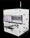
The research and development of equipment is extremely challenging. The domestic technical foundation in this field is relatively weak and it has long relied on foreign imports. Electronic Technology Equipment China Electronic Technology Fenghua Company has successfully made breakthroughs in key core technologies for optical inspection such as laser scattering and microscopic imaging. It adopts an automatic defect detection algorithm based on deep learning. Wafer inspection and data analysis can be processed in parallel, and defect location is related to device failure. Connected to meet the needs of production inspection and yield improvement of multi-size SiC wafers. This equipment has the advantages of high-resolution imaging, low noise, high detection throughput, high detection rate, and high accuracy. Its technical level has reached the international advanced level, and it has the mass production capacity and engineering application level of the whole machine. It has obtained many awards. Batch application and wide recognition by leading customers in the industry.
It is understood that in the next step, Dianke Fenghua Company will adhere to long-termism, keep up with the development of advanced processes, promote iterative upgrades and mass production applications of SiC wafer defect detection equipment, lead the development of new quality productivity with innovative momentum, and effectively promote The supply chain of the third-generation semiconductor industry chain is optimized and upgraded.
ASMPT and Aoximing Exhibit Advanced Semiconductor Equipment
Today, Aoxin Bright, a leading domestic semiconductor equipment supplier, will attend SEMICON China 2024. As part of the ASMPT global technology network, Aoxinming participated in this SEMICON China for the first time as a Chinese equipment manufacturer. At this exhibition, Aoximing and ASMPT demonstrated a variety of advanced equipment for high-quality and high-precision chip packaging in Hall N3.
SEMICON China is an industry event covering the entire industry chain and the largest and most influential industry exchange event in the world. This year's SEMICON China focuses on the global industrial landscape, cutting-edge technologies and market trends, and gathers upstream and downstream industry experts to discuss the characteristics of China's semiconductor industry and global development trends.
Xu Zhiwei, CEO of Aoxinming, said: "Driven by AI and automotive electronics, the industry's demand for high-performance chips is further rising, and the pace of chip localization will be further accelerated. Aoxinming adheres to 'advanced technology, endows In line with China Chip's brand purpose, we are accelerating the layout of local R&D centers and incubating high-end equipment that is more in line with local needs."
Aoxinming was formally established in August 2023. It is an enterprise established by ASMPT to meet the needs of Chinese semiconductor manufacturing companies. By combining ASMPT's international leading technology and local technology and processes, Aoxinming is committed to providing domestic and foreign chip and packaging manufacturers with High quality, localized, and competitive overall solution. As an independent entity in China, Aoxinming will implement 100% localization in all aspects of the supply chain, assembly, design and services, which will ensure that it can respond to the needs of local customers faster and better serve the Chinese market.
At present, Aoxinming has completed the design of the first domestic R&D center and is expected to be unveiled in mid-2024. The R&D center has a total area of approximately 7,000 square meters and is located in Shanghai Lingang New Area.
At this year's SEMICON China, Aoximing and ASMPT jointly demonstrated Eagle AERO, Photon Pro, LA-PRO, LOTUS12 and other advanced equipment. Eagle AERO is an advanced welding technology equipment in the industry, with efficient and excellent welding capabilities. Photon Pro is an automated high-precision die bonding equipment with high flexibility in options. It can handle various multi-wafer packaging requirements, and can automatically switch welding and wafer switching to achieve high-precision die bonding. LA-PRO is a fully automated lens mount welding system that can weld and look up optics with 4-megapixel image resolution for precise placement. LOTUS12 is a fully automatic die-bonding machine with high flexibility, which can improve the die-bonding speed and placement accuracy, intelligently switch the viewing range and high-resolution camera modules, and has packaging processing capabilities to cope with different market positioning.
Guangyan Technology completed tens of millions of Pre-A rounds of financing
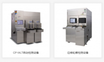
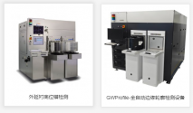
Recently, Hangzhou Guangyan Technology Co., Ltd. completed tens of millions of Pre-A rounds of financing, jointly completed by Shenzhen Hi-tech Investment and Haifu Industrial Fund. This round of financing will be used for the R&D and production of 300mm silicon wafer defect detection equipment for integrated circuits and the creation of a talent team.
Hangzhou Guangyan Technology Co., Ltd. was established in 2022. It is a high-tech enterprise focusing on the research and development, production and sales of semiconductor wafer inspection equipment. The company is located in the Hangzhou Integrated Circuit Industrial Park. The factory has a R&D laboratory of more than 1,000 square meters and a clean workshop of 500 square meters, which is used for the R&D, manufacturing and sample testing of defect detection equipment for silicon wafers for integrated circuits.
Liu Ao, general manager of Xiamen Fund of Shenzhen High-tech Investment Group, said: "Silicon substrate wafer is the most important upstream link in the semiconductor industry chain. The quality of silicon wafers directly determines chip performance. At a time when domestic substitution in the semiconductor industry is in full swing, targeting defects in 300mm silicon wafers Most high-end testing equipment is still monopolized by European, American and Japanese manufacturers, and domestic equipment is in urgent need of breakthroughs. Guangyan Technology has strong R&D strength and deep technical accumulation. A variety of wafer testing equipment has been shipped in batches to domestic leading customers, breaking the foreign technology blockade. , to help the development of China's semiconductor industry. Hi-tech Investment is very optimistic about the future development of Optical Research Technology and will accompany the company's growth for a long time. We look forward to it becoming an industry benchmark enterprise as soon as possible!"
Zhang Junyu, general manager of Haifu Industrial Investment Fund Management Co., Ltd., said: "At this stage, domestic large silicon wafers have achieved a breakthrough from 0 to 1. In order to continue to improve their competitiveness and profitability in the future, silicon wafer factories will inevitably need to increase the output of positive wafers. shipment ratio, and break through the large silicon wafer production capacity used to manufacture advanced process ICs. In this process, silicon wafer factories will continue to have strong demand for defect detection equipment. We look forward to Hangzhou Optical Research's deep technological accumulation through the team, enriching Our experience in the semiconductor equipment industry will help the development of the domestic large silicon wafer industry and promote the localization process of the semiconductor quality testing equipment industry."
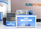
Shanghai Xianpu Gas Technology Co., Ltd. releases new gas filter.
Recently, during Semicon China 2024, Shanghai Xianpu Gas Technology Co., Ltd. held a high-profile "high-efficiency, precise, nanoscale" Xianpu gas filter new product launch conference. The conference attracted many experts, customers and media representatives from the semiconductor industry.
The gas filter is an innovative product launched by Shanghai Xianpu Gas Technology Co., Ltd. after a long period of research and development and testing. Through four filtration mechanisms: screening, direct interception, inertial influence and diffusion interception, it can achieve high efficiency, precision and nano-level filtering. The filtration effect effectively improves the gas purity and quality in the semiconductor production process.

Xianpu was established in Shanghai in 2004. The founder team has 40 years of experience in the semiconductor industry and 20 years of experience in R&D, manufacturing and service of 9N gas purification equipment. Xianpu has experienced 20 years of localization, holds 60 national patents, and independently developed More than a dozen series and hundreds of products, including POU gas purifiers used in semiconductor process equipment and gas purification equipment used in semiconductor chip factories, combine gas purification solutions with practical applications to solve gas purification problems for customers in the semiconductor industry. solve the problem and realize the domestic replacement of 9N gas purifier. As Xianpu gas filters are introduced to the market, Xianpu has solved another "stuck neck" problem in the domestic chip industry by combining its strong engineering capabilities and rich industry experience with the domestic current situation.
Dr. Jiang Xiaosong, chairman and general manager of Shanghai Xianpu Gas Technology Co., Ltd., said that the company will continue to increase investment in research and development of products related to the gas micro-pollution control industry, continuously optimize services, provide customers with better solutions, and strive to contribute to China’s semiconductor industry. Make a greater contribution.
Yin Zhiyao: Most of China Micro's etching equipment components have been domestically produced!
On March 19, Yin Zhiyao, chairman and general manager of China Microelectronics Corporation, a major domestic semiconductor equipment manufacturer, stated at the 2023 annual performance briefing that most of the components of Microelectronics' etching equipment have been domestically produced, and in a very short time Within a certain period of time, the foundation of independent control will be fully realized.
Under the current international situation where the import of related semiconductor equipment and parts is restricted, the substitution of related imported parts has become an important issue for the development of Sinomicron.
At the performance briefing of last year's semi-annual report, Yin Zhiyao said that since the United States strengthened export controls in October last year to cut off the connection between Chinese manufacturing plants and American advanced tools, Chinese customers have accelerated the adoption of AMEC's etching equipment.
Affected by this, AMEC's market share in the capacitively coupled plasma (CCP) etching equipment market is expected to increase from 24% in October 2022 to 60% in June 2023. As for the inductively coupled plasma (ICP) equipment market, after the once-dominated U.S. Lam Semiconductor's market share has dropped significantly, AMEC's market share may rise from almost zero to 75%.
Yin Zhiyao predicted at that time that 80% of China Micro's restricted imported parts could be replaced domestically by the end of 2023, and 100% replacement would be achieved in the second half of 2024.
Judging from the time progress, in just over half a year, most of the etching equipment components of AMEC have been domestically produced, which is extremely fast! It should be pointed out that this "caliber" includes not only " restricted imported parts ", but also includes unrestricted imported parts. This also means that the degree of localization and controllability of China's micro-etching equipment has been greatly improved.
Photonic computing chip company Light-based Technology completed nearly 100 million yuan in angel+ round of financing
Recently, photonic computing chip OPU manufacturer Light-based Technology (Suzhou) Co., Ltd. (hereinafter referred to as "Light-based Technology") completed nearly 100 million yuan in angel + round financing. This financing was led by Zhongying Venture Capital, with participation from Relay Angel and Mushi Capital. Old shareholders Xiaomiao Langcheng and Fengrui Capital also invested in excess of the amount.
Light-based technology was established in April 2022. The team is composed of senior experts from the University of Oxford, Fudan University, University of Chicago, and optical communications, computing chips and other fields. It aims to develop photon computing products with high computing power and low power consumption, and provide services. Based on AI reasoning and training scenarios in the era of large models, it creates a computing power paradigm in the era of digital intelligence.The PCM+Crossbar route adopted by the optical standard is a storage and calculation integrated optical computing chip based on phase change materials, which has the advantages of low power consumption, small size, and low packaging difficulty. Optical Technology's OPU (Optical Processing Unit) chip maintains rapid iteration and has completed three tape-outs so far. The interfaces and instruction sets in the product form are highly compatible with existing data centers, and future chips can also be adapted to large models on the market.
Light-based technology was established in April 2022. The team is composed of senior experts from the University of Oxford, Fudan University, University of Chicago, and optical communications, computing chips and other fields. It aims to develop photon computing products with high computing power and low power consumption, and provide services. Based on AI reasoning and training scenarios in the era of large models, it creates a computing power paradigm in the era of digital intelligence.The PCM+Crossbar route adopted by the optical standard is a storage and calculation integrated optical computing chip based on phase change materials, which has the advantages of low power consumption, small size, and low packaging difficulty. Optical Technology's OPU (Optical Processing Unit) chip maintains rapid iteration and has completed three tape-outs so far. The interfaces and instruction sets in the product form are highly compatible with existing data centers, and future chips can also be adapted to large models on the market.
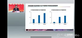
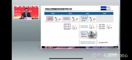
AMEC is making great progress as per @tokenanalyst link. This is their presentation on where they are coverage wise for etching tools in advanced memory process currently and also the product development plants for deposition tools
