Chinese semiconductor thread II

tokenanalyst

Lieutenant General
Registered Member

The world's first 8.6th generation AMOLED production line equipped with FMM-free technology held a ceremony to mark the installation of its process equipment.​


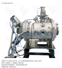
On April 15, 2026, Hefei Guoxian Technology Co., Ltd. marked a significant milestone by successfully moving the first exposure machine into the cleanroom of its new production facility. This event signifies the transition from the construction phase to equipment installation and commissioning for what is being hailed as the world's first 8.6th generation AMOLED line equipped with FMM-free (ViP) technology. The successful integration of this core process equipment lays a solid foundation for subsequent product lighting, mass production delivery, and the realization of higher-end display capabilities globally.

The project has progressed at an unprecedented pace, demonstrating remarkable efficiency from its inception. With civil construction beginning in February 2025, the main plant was topped out in just 168 days—a record speed for high-generation lines—and underwent rigorous cleaning in March 2026 to prepare for equipment relocation. ViP technology has already proven its industrial viability through a successful supply contract with Honor for wearable products, earning unanimous praise from leading experts at the Chinese Academy of Sciences who rated it as internationally advanced. With a total investment of 55 billion yuan and a monthly capacity of 32,000 glass substrates, the line is designed to produce panels ranging from micro to large sizes, supporting diverse applications including flat and 3D displays.

Looking ahead, this production line aims to capitalize on the growing "AI + Display" wave by powering next-generation devices such as AI smartphones, PCs, smart cars, and emerging smart robot markets. By leveraging ViP's high brightness, low power consumption, and long lifespan, Hefei Guoxian intends to expand OLED penetration into new sectors while advancing China's display industry toward independent innovation and high-quality development. As the line accelerates toward full-scale industrialization, it represents a strategic effort to empower customers with superior technology, ensuring that Chinese screens can successfully compete globally in both consumer electronics and emerging fields.

Please, Log in or Register to view URLs content!
 

tokenanalyst

Lieutenant General
Registered Member

Jingsheng Mechanical & Electrical: 12-inch silicon carbide substrate samples sent for verification; 8-inch substrates secure bulk orders from both domestic and international markets.​


Jingsheng Mechanical & Electrical has announced significant breakthroughs in its third-generation semiconductor strategy, marking a pivotal advancement for the "equipment + materials" synergy model. The company successfully developed a fully domestic 12-inch silicon carbide substrate processing pilot line with all equipment sourced locally. Samples from this new facility have been sent to downstream customers for verification, representing a crucial step toward industrializing large-scale production that promises to increase chip output by approximately 2.25 times and reduce unit costs by about 40%.


In the realm of manufacturing tools, Jingsheng has overcome high technological barriers to secure market penetration in advanced epitaxial growth equipment. Both its 12-inch atmospheric pressure and reduced pressure systems have achieved sales and repeat purchases from key customers, featuring international-level indicators and sophisticated multi-zone temperature control.
Furthermore, the company has secured orders for a comprehensive suite of 8–12 inch supporting equipment, including oxidation furnaces and ion implantation tools, which are currently undergoing customer verification to support future mass production capabilities.
1776266396970.png
On the commercial front, the company's 6–8 inch silicon carbide substrates have achieved large-scale mass production with industry-leading core parameters, securing bulk orders from both domestic and international markets. While 12-inch optical-grade substrates have reached small-batch production for emerging applications like AR/VR, the primary focus remains on expanding the global supply chain through a dual "domestic + overseas" capacity layout. The Yinchuan base in China has officially begun producing 8-inch supporting crystals, while an industrialization project in Penang, Malaysia, is currently under construction to strengthen global distribution.

Looking ahead, these simultaneous breakthroughs across equipment and materials positions Jingsheng as a leading Chinese enterprise capable of reducing reliance on foreign technology. As demand for silicon carbide surges in sectors like new energy vehicles, photovoltaic inverters, and industrial power supplies, the company is poised to capitalize on industry trends toward larger wafer sizes and lower costs. This strategic expansion aims not only to solidify its leadership but also to propel China's third-generation semiconductor industry into a new stage of widespread commercialization.​

Please, Log in or Register to view URLs content!
 

Michael90

Senior Member
Registered Member
YMTC fab 2 already has fully domestic production line. News of fab 3 completing construction appeared on local newspaper in Jan & likely they will use mostly domestic tools if not all.

just yesterday Reuters break the exclusive information. YMTC adding two more fabs besides their fab3 in Wuhan. same CXMT is doing and adding additional capacity.

self-reliance goal has almost achieved in Memory. memory is one of the industry where Chinese players are close to leading edge right now obviously alongside other top players like Hynix and SS.
-----------------------------------------------------------------------------------------------------------
YMTC is leader in Hybrid Bonding Tech. its also called ''Xtacking'' and Samsung reportedly signed a patent licensing agreement with YMTC for 400 layers Flash memory.

Please, Log in or Register to view URLs content!

Please, Log in or Register to view URLs content!
-------------------------------------------------------------------------------------------------------------

the conclusion is, YMTC/CXMT rapidly gaining market share with keep adding additional capacity that too using local tools/equipment.

But dominance ? not yet but that is not quite far off.
The thing is that china has already made self sufficiency in semi conductors a national priority in her 5 year plans . So by the end d of this latest 5 year plan, I'm 100% sure they would have achieved self sufficiency in almost all those crucial semiconductor sectors , maybe with some minor exceptions. That's the most important, since once Chinese semiconductor companies and equipment makers dominate chinas market, they will automatically be among the top if not the top globally in their category , since china has the worlds largest semiconductor market by far. From dominating chinas market they will gain scale , experience , and learn from the feedback loop of their equipments and procuts being used on a maas scale , which will help them expand abroad and gain market share progressively globally. It's happened to many other sectors in the past, this won't be any different. Just a matter of time.
To be honest US sanctions in this sector has been a boon for the CCP, since they were trying to entice private Chinese companies and even some state ones to give priority or a chance to Chinese semiconductor companies in the past but these companies never listened nor wanted to do so, due to obvious reasons as foreign semi companies were more advanced /proven than local ones. So most Chinese semi companies were marginalized and never given a chance to even start proving themselves and getting their products tested in real life situations(something that's crucial for companies in this sector to fine tune their products ). US sanctions changed all this , and forced local companies from giving a chance to local players . So in some ways the US governemtn aided the Chinese government objectives immensely . This can't be overstated enough.
 

tokenanalyst

Lieutenant General
Registered Member

Jinhong Gas has signed a contract with a major international memory chip manufacturer to supply ultra-high purity nitrous oxide (N₂O) gas.​

Jinhong Gas recently signed a formal gas supply framework contract with a major international memory chip industry player, becoming one of its direct gas suppliers. According to the agreement, Jinhong Gas will supply ultra-high purity nitrous oxide (N₂O) gas to this international memory chip company. This type of gas is mainly used in the chemical vapor deposition (CVD) process of semiconductor manufacturing, and has extremely high requirements for purity and stability. This signing represents a strategic breakthrough for Jinhong Gas in the field of semiconductor electronic specialty gases.

Please, Log in or Register to view URLs content!
 

tokenanalyst

Lieutenant General
Registered Member

MicroNano equipment has shipped over 6 million wafers.​


Behind the technological breakthrough lies strong market validation. In just three years, MicroNano's equipment has shipped over 6 million wafers. From technology validation to large-scale mass production, MicroNano has prioritized speed and quality, winning the market with high performance, high stability, and high reliability, marking the company's ALD and CVD equipment as having fully entered the large-scale mass production stage.

In 2025 , the company's semiconductor equipment revenue reached 881 million yuan, a year-on-year increase of 169.12% , and its share of main business revenue jumped from 12.14% to 33.50% . The semiconductor business is becoming the core engine driving the company's growth.

MicroNano is demonstrating its leading position in the semiconductor thin-film deposition equipment market with its full-scenario product matrix, differentiated technology positioning, and large-scale verification capabilities . In the future, MicroNano will continue to uphold its commitment to innovation, continuously break through core technologies, and resonate and collaborate with industry trends in logic , memory, and advanced packaging to inject strong momentum into the self-reliance and controllability of China's domestic semiconductor industry chain.

High-k ALD equipment for 28nm front-end production line. Its new generation iTomic® PE employs unique Thunder Balance® technology, enabling millisecond-level switching of RF effects.

1776289662023.png

In the technological evolution of DRAM memory chips , filling high aspect ratio structures has become a core challenge for the industry. To address this challenge, MicroNano has developed the iTomic® SPX series of spatial atomic layer deposition (ALD) equipment, which specifically solves this industry problem.
1776289814926.png

Micro-Nano Layout targets the emerging market driven by AI computing power . Addressing the extremely thermally sensitive process requirements in 2.5D/3D packaging, the company has pioneered the iTronix® series of low-temperature PECVD equipment .

1776289904960.png

Please, Log in or Register to view URLs content!
 

sunnymaxi

Colonel
Registered Member

MicroNano equipment has shipped over 6 million wafers.​


Behind the technological breakthrough lies strong market validation. In just three years, MicroNano's equipment has shipped over 6 million wafers. From technology validation to large-scale mass production, MicroNano has prioritized speed and quality, winning the market with high performance, high stability, and high reliability, marking the company's ALD and CVD equipment as having fully entered the large-scale mass production stage.

In 2025 , the company's semiconductor equipment revenue reached 881 million yuan, a year-on-year increase of 169.12% , and its share of main business revenue jumped from 12.14% to 33.50% . The semiconductor business is becoming the core engine driving the company's growth.

MicroNano is demonstrating its leading position in the semiconductor thin-film deposition equipment market with its full-scenario product matrix, differentiated technology positioning, and large-scale verification capabilities . In the future, MicroNano will continue to uphold its commitment to innovation, continuously break through core technologies, and resonate and collaborate with industry trends in logic , memory, and advanced packaging to inject strong momentum into the self-reliance and controllability of China's domestic semiconductor industry chain.

High-k ALD equipment for 28nm front-end production line. Its new generation iTomic® PE employs unique Thunder Balance® technology, enabling millisecond-level switching of RF effects.

View attachment 173518

In the technological evolution of DRAM memory chips , filling high aspect ratio structures has become a core challenge for the industry. To address this challenge, MicroNano has developed the iTomic® SPX series of spatial atomic layer deposition (ALD) equipment, which specifically solves this industry problem.
View attachment 173519

Micro-Nano Layout targets the emerging market driven by AI computing power . Addressing the extremely thermally sensitive process requirements in 2.5D/3D packaging, the company has pioneered the iTronix® series of low-temperature PECVD equipment .

View attachment 173520

Please, Log in or Register to view URLs content!
look at the jump in revenue.

these are Tier2 companies in semiconductor manufacturing equipment. there is still large imbalance in demand and supply so these mid sized companies can fulfil the gap alongside Big players.
 

tokenanalyst

Lieutenant General
Registered Member
Lot of companies new and old expanding their profile on EUV technologies in China. Runli Vacuum expanded their Vacuum manufacturing and R&D capabilities with a new facility in 2023

High End Vacuum EUV light source testing platform.

1776292758644.png

Shanghai Runli Vacuum Technology Co., Ltd. (hereinafter referred to as "Runli Vacuum"), founded in June 2016, is a high-tech enterprise specializing in the research and development, design, production, technical services and after-sales services of vacuum and cryogenic equipment.
Headquartered in Jindi Weixin Baoshan Intelligent Manufacturing Park, Baoshan District, Shanghai, the company has 1,500 square meters of R&D and office space. To enhance its manufacturing capabilities for large-scale, high-precision equipment, Runli Vacuum established a new production base in Liuhe Town, Taicang City, Suzhou in 2023 – Runli (Suzhou) Vacuum Technology Co., Ltd.

Ultra-large manufacturing space: with a total building area of 7,942 square meters, the Suzhou factory has a single-story height of 14 meters, providing key resource guarantees for the manufacturing of large equipment.

Heavy-duty precision machining capabilities: The base is equipped with a large gantry machining center and an ultra-large welding platform to ensure the machining accuracy and stability of large and complex structural parts.

Overall Manufacturing Capability for Ultra-Large Vacuum Chambers: Leveraging the aforementioned high-specification workshops and heavy equipment, we have established the capability to process and manufacture ultra-large vacuum chambers exceeding 10 meters in length. This capability effectively addresses the key challenges of manufacturing precision, structural integrity, and sealing in large vacuum systems.

Please, Log in or Register to view URLs content!
 

Attachments

  • 1776292206120.png
    1776292206120.png
    569.7 KB · Views: 7

tokenanalyst

Lieutenant General
Registered Member
look at the jump in revenue.

these are Tier2 companies in semiconductor manufacturing equipment. there is still large imbalance in demand and supply so these mid sized companies can fulfil the gap alongside Big players.
Correct. Microguide Nano is pretty big in the photovoltaic sector in which they sell a lot of ALD tools from there they expanded into packaging but they saw a big boom after the US expanded their exports controls after 2019, but as the big players like Naura, AMEC and Piotech expand the portafolios they are becoming "a fill the gaps kind of company"
 

Clark Gap

Junior Member
Registered Member
Lot of companies new and old expanding their profile on EUV technologies in China. Runli Vacuum expanded their Vacuum manufacturing and R&D capabilities with a new facility in 2023

High End Vacuum EUV light source testing platform.

View attachment 173522

Shanghai Runli Vacuum Technology Co., Ltd. (hereinafter referred to as "Runli Vacuum"), founded in June 2016, is a high-tech enterprise specializing in the research and development, design, production, technical services and after-sales services of vacuum and cryogenic equipment.
Headquartered in Jindi Weixin Baoshan Intelligent Manufacturing Park, Baoshan District, Shanghai, the company has 1,500 square meters of R&D and office space. To enhance its manufacturing capabilities for large-scale, high-precision equipment, Runli Vacuum established a new production base in Liuhe Town, Taicang City, Suzhou in 2023 – Runli (Suzhou) Vacuum Technology Co., Ltd.

Ultra-large manufacturing space: with a total building area of 7,942 square meters, the Suzhou factory has a single-story height of 14 meters, providing key resource guarantees for the manufacturing of large equipment.

Heavy-duty precision machining capabilities: The base is equipped with a large gantry machining center and an ultra-large welding platform to ensure the machining accuracy and stability of large and complex structural parts.

Overall Manufacturing Capability for Ultra-Large Vacuum Chambers: Leveraging the aforementioned high-specification workshops and heavy equipment, we have established the capability to process and manufacture ultra-large vacuum chambers exceeding 10 meters in length. This capability effectively addresses the key challenges of manufacturing precision, structural integrity, and sealing in large vacuum systems.

Please, Log in or Register to view URLs content!
We actually had them custom-build a few systems for us. They mentioned moving from their old plant in Baoshan to a new one in Taicang — now I see that's what it was for.
 
Top