Since its 2024 I approved his message.if i remember, you said on twitter. SMIC will become second largest pure fab in the world in 2025..
You are using an out of date browser. It may not display this or other websites correctly.
You should upgrade or use an alternative browser.
You should upgrade or use an alternative browser.
Chinese semiconductor thread II
- Thread starter vincent
- Start date
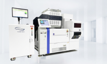
Guangli Microelectronics enriches its electrical testing product matrix and launches T4000 Max 100pin multi-channel parallel parameter testing machine
Electrical testing equipment plays an important role in the process development, product introduction and mass production of integrated circuits. By increasing the speed of test equipment, new product development cycles can be accelerated, production efficiency can be improved, and testing costs can be reduced. This not only helps bring new design chips to the market quickly, but also has a positive impact on the entire chip production process and promotes the sustainable development of the chip industry.
T4000 Max comes out and testing speed is greatly improved
Recently, Guangli Microelectronics launched the T4000 Max semiconductor parameter test machine, which is configured with 100 pins and supports multi-channel parallel testing, which can better serve customers with multiple test items and high test efficiency requirements. T4000 Max (100pin) enriches the matrix of Canton Micro’s typical test products and further expands the company’s high-speed high-end test machine categories, marking another important achievement achieved by Canton in the cutting-edge field of wafer-level electrical test equipment.
The T4000 Max (100pin) series adopts a self-developed high-performance matrix switch architecture , which has the characteristics of high precision, fast speed, and flexible configuration. It is suitable for various test scenarios such as process research and development, wafer-level reliability, and mass production WAT.

HBM?
Changxin Memory applies for a patent for wafer-level packaging method to improve the yield of wafer packaging
According to the announcement from the State Intellectual Property Office, Changxin Storage Technology Co., Ltd. applied for a project called "Wafer Level Packaging Method", with the public number CN117690804A, and the application date is September 2022.
The patent abstract shows that embodiments of the present disclosure provide a wafer-level packaging method, which includes: providing a wafer; forming an electrical connection structure in the wafer, the bottom of the electrical connection structure is located in the wafer, and the top surface of the wafer exposes the electrical connection structure Top; form a chip on the wafer, and the chip is in electrical contact with the top of the electrical connection structure; form a packaging structure on the wafer, and the chip is located in the packaging structure; perform a first back grinding process on the bottom surface of the wafer to expose the bottom of the electrical connection structure ; Form a conductive structure, and the conductive structure is in contact with the bottom of the electrical connection structure. The embodiments of the present disclosure are at least beneficial to improving the yield of wafer packaging.
The patent abstract shows that embodiments of the present disclosure provide a wafer-level packaging method, which includes: providing a wafer; forming an electrical connection structure in the wafer, the bottom of the electrical connection structure is located in the wafer, and the top surface of the wafer exposes the electrical connection structure Top; form a chip on the wafer, and the chip is in electrical contact with the top of the electrical connection structure; form a packaging structure on the wafer, and the chip is located in the packaging structure; perform a first back grinding process on the bottom surface of the wafer to expose the bottom of the electrical connection structure ; Form a conductive structure, and the conductive structure is in contact with the bottom of the electrical connection structure. The embodiments of the present disclosure are at least beneficial to improving the yield of wafer packaging.
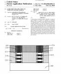
I don't think this is necessarily SMIC's 3nm process. If I'm reading this right it's just for SMIC's GAA transistor architecture, which is might not be specific to the node that SMIC is working toward. Also, between this and Huawei's improved Finfet and rumours of CFET being worked towards I think whatever might become of SMIC's 3nm node is unclear.SMIC "3nm" US patent application.
View attachment 126563
The patent application doesn't mention EUV so maybe they are mostly reliant of multi-patterning techniques and ALD and ALE for making the transistors.
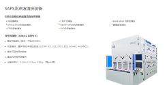
Shengmei Shanghai wet method equipment 4000 cavities were successfully delivered.
4000 cavities of Shengmei Shanghai wet method equipment were successfully delivered. Shengmei Shanghai successfully delivered 2,000 cavities of wet process equipment in October 2021, and exceeded 3,000 cavities in November 2022. Now the milestone of 4,000 cavities has been reached. According to Shengmei Shanghai news, Wang Jian, general manager of Shengmei Shanghai, said: "Shengmei's cleaning equipment can perform logic and storage for more than 90% of the cleaning processes. We can expect that the wet method equipment will soon exceed 5,000 cavities."
Shengmei Semiconductor Equipment (Shanghai) Co., Ltd. was established in 2005. It is an integrated circuit equipment enterprise introduced by the Shanghai Municipal Government’s project to rejuvenate the city through science and education. It integrates R&D, design, manufacturing and sales to provide high-end semiconductor equipment to customers around the world. The main products include single wafer and tank wet cleaning equipment, electroplating equipment, stress-free polishing equipment, vertical furnace tube equipment, front-end coating and development equipment, and PECVD equipment.

This mean we will see a prototype EUVL machine within the Year.
SMIC Rumored To Be Setting Up An Internal Research And Development Team To Kick Off Work On The 3nm Process Within The Year
•Mar 11, 2024 03:21 AM EDT
•Copy Shortlink
After SMIC was reportedly setting up chip production for Huawei to later this year, China’s biggest semiconductor manufacturer is now rumored to be assembling a team dedicated to 3nm chip development. For obvious reasons, the company will seek aid to help achieve this monumental goal and, in the process, obtain complete autonomy from foreign companies and the tight grip that the U.S. has on them.
SMIC said to seek subsidies from the Chinese government to help it reach its goal of mass production of 3nm wafers
As reported by DigiTimes, Joongang mentions that SMIC’s initial goal is to begin operations of its 5nm production line that will not just mass produce Huawei chipsets for a wide range of products but also AI silicon. It is reported that the Chinese manufacturer will accomplish this using the existing DUV machinery that it will likely re-purpose since ASML, the only company in the world that can supply cutting-edge EUV technology, has been barred from supplying this equipment to not just SMIC but any company of Chinese origin.
However, SMIC is looking beyond the 5nm threshold, just as it did when it partnered with Huawei to launch the 7nm Kirin 9000S. The latest report states that the semiconductor maker has formed an internal research and development team that will commence work on the 3nm node. One of the biggest obstacles standing in the way of SMIC’s goal is low yields and high production costs, but the company is said to have a strategy that involves receiving massive subsidies from the Chinese government.
Receiving subsidies will be of paramount importance to SMIC, especially given that an earlier report stated that its than TSMC’s on the same manufacturing process due to using the older DUV equipment. However, we do not expect the first 3nm wafers from the company to roll out until after a few years. For starters, commercialization of Huawei’s 5nm chips will be given priority, and it is possible that this technology will be utilized for a few years before we witness a transition to the realm of 3nm wafers. Whatever decision SMIC will take, one thing is clear; this will be the most challenging task undertaken by the company.
I think SMIC still gonna use DUV to tackle 3nm.
using computational lithography technique. Special layout to overcome the limitation.
I could be or could be no, but is an US patent, so SMIC is giving a lot importance to this process.I don't think this is necessarily SMIC's 3nm process. If I'm reading this right it's just for SMIC's GAA transistor architecture, which is might not be specific to the node that SMIC is working toward. Also, between this and Huawei's improved Finfet and rumours of CFET being worked towards I think whatever might become of SMIC's 3nm node is unclear.
Shanghai Xinyang’s net profit in 2023 is 167 million yuan! A year-on-year increase of 213.41%.
On the evening of March 11, Shanghai Xinyang disclosed its 2023 performance report. The company's revenue for that year was 1.212 billion yuan, a year-on-year increase of 1.40%; the net profit attributable to the parent company was 167 million yuan, a year-on-year increase of 213.41%.
Shanghai Xinyang said that during this reporting period, the company achieved operating income of 1.212 billion yuan, a slight increase compared with the same period last year. The net profit attributable to shareholders of listed companies was 167 million yuan, a year-on-year increase of 213.41%. The net profit after deducting non-recurring gains and losses was 123 million yuan, a year-on-year increase of 10.27%.Among them, the semiconductor business grew by 20.06%, the market share of electroplating solutions and additive series products for wafer manufacturing increased rapidly, and the cleaning series products for integrated circuit manufacturing were successfully certified by the client, and sales grew rapidly. For the paint segment business, affected by unfavorable factors such as the sluggish market environment in the construction industry and the sharp drop in selling prices of paint products, operating income fell by 20.08% compared with the same period last year.
Shanghai Xinyang said that during this reporting period, the company achieved operating income of 1.212 billion yuan, a slight increase compared with the same period last year. The net profit attributable to shareholders of listed companies was 167 million yuan, a year-on-year increase of 213.41%. The net profit after deducting non-recurring gains and losses was 123 million yuan, a year-on-year increase of 10.27%.Among them, the semiconductor business grew by 20.06%, the market share of electroplating solutions and additive series products for wafer manufacturing increased rapidly, and the cleaning series products for integrated circuit manufacturing were successfully certified by the client, and sales grew rapidly. For the paint segment business, affected by unfavorable factors such as the sluggish market environment in the construction industry and the sharp drop in selling prices of paint products, operating income fell by 20.08% compared with the same period last year.

