Chinese semiconductor thread II

tphuang

General
Staff member
Super Moderator
VIP Professional
Registered Member
I don't believe we are at a point where the electricity cost is actually all that important. From what I can tell, the biggest issue with the electric grid in U.S. is capacity and access.

For example, as you all exhaustively know and poke fun at, the actual act of building something in America, is a years long process. Not just the actual concrete-pouring, but the permitting, regulations, political handshaking, etc.

The way in which some of these things are mitigated, is by finding areas where the regulatory process can be "speedrun". The problem, is that this goldilocks area where the regulatory process can be sped up, but also has the available electricity capacity is fairly limited. This is why things like this modular, deployable gas generator got so much hype. Because it allows data centers to be potentially built in the middle of nowhere, as fast as possible.

Cost, isn't a problem or a bottleneck for these companies. China's electricity advantage will take far more time to materialize. Possibly after the AI bubble bursts in America (assuming it does). Currently, the industry is just not that price sensitive.

Please, Log in or Register to view URLs content!

guys, this is getting way off topic. Anything more on the electricity and cost advantage category will get deleted.

You can continue to talk about this stuff in AI thread if you want.
 

tonyget

Senior Member
Registered Member

China Reaches New Semiconductor Milestone as TechInsights Confirms First Commercial STT-MRAM Shipments​

Please, Log in or Register to view URLs content!

Over the coming weeks TechInsights will continue to undertake detailed and complete technical analysis of the STT-MRAM Chip.

China’s semiconductor industry has taken a major step forward. TechInsights analysis confirms that Shanghai Siproin Microelectronics 上海矽朋微 is now shipping commercial STT-MRAM chips, marking the first commercially available emerging memory technology produced in China.

This breakthrough positions China as a growing contender in the global MRAM market, with Siproin’s devices targeting embedded, IoT, industrial, and automotive applications that require fast, durable, non-volatile memory. The commercial release also suggests that Chinese foundries—likely SMIC—have successfully mastered the complex manufacturing processes behind STT-MRAM, a significant technical achievement.

Siproin’s progress strengthens China’s broader memory push, joining CXMT’s DRAM and YMTC’s 3D NAND to form an increasingly complete domestic memory ecosystem. The timing is critical as U.S. export controls accelerate China’s drive for semiconductor independence.

For major global memory vendors such as Samsung, Micron, SK hynix, and Everspin, the emergence of commercial Chinese MRAM introduces new competition in sectors governments consider high priority, including industrial control systems and IoT edge devices.

TechInsights’ analysis shows that the performance gap between Chinese MRAM and leading global manufacturers is narrowing, with functional parity possible within 3–5 years given China’s scale, investment, and momentum.
 

tokenanalyst

Lieutenant General
Registered Member

Hongce Optoelectronics has obtained a patent for a LaNx/La/B4C extreme ultraviolet multilayer mirror and its fabrication method.​


According to information from the State Intellectual Property Office, Suzhou Hongce Optoelectronic Technology Co., Ltd. has obtained a patent entitled "A LaNx/La/B4C Extreme Ultraviolet Multilayer Film Reflector and Its Preparation Method", with authorization announcement number CN116107001B and application date of December 2022.

The company is dedicated to the research and development and production of precision optical nanofilm devices and PVD coating equipment, covering a wavelength range of infrared, visible light, deep ultraviolet (DUV), vacuum ultraviolet (VUV), extreme ultraviolet (EUV), X-ray, and neutron. In the short-wavelength optical thin film fields of extreme ultraviolet, X-ray, and neutron optics, we have overcome key core technologies in the development of nanostructure thin film devices and equipment, achieving domestic production. We are a high-tech company integrating R&D, production, and sales. Benchmarking against ASML (Netherlands) and Zeiss (Germany) international extreme ultraviolet lithography machines, we focus on solving the bottleneck technologies in advanced process extreme ultraviolet (EUV) lithography machines. We have independently developed high-precision, large-size PVD coating equipment for lithography machines, achieving the first set. We have also overcome the process of preparing multi-layer thin film mirrors for extreme ultraviolet light, achieving mass production of large-aperture, high-reflectivity extreme ultraviolet mirrors; and achieving full-process independent control of key EUV thin film components.


tokenanalyst

Lieutenant General
Registered Member

Gazer optical metrology equipment company completes 100 million yuan strategic financing!​


According to news from the company's official WeChat account, Gaize Technology, a leading domestic semiconductor technology company, recently completed a strategic financing round of nearly 100 million RMB. This round was led by well-known industrial investment institution Jinyu Maowu, with existing shareholders Suzhou High-tech Financial Holdings and Suzhou Venture Capital Group also participating.

The funds raised in this round of financing will be primarily used for continuous technological iteration of existing products, capacity expansion, and R&D investment in next-generation technologies.

Gaize Technology is deeply rooted in the field of industrial automation, focusing on the research and innovation of sensing and control technologies. Its products are widely used in lithium battery production, new energy manufacturing, 3C production, health and medical care and other fields.

In the semiconductor field, the company has quietly become an "invisible champion" in the semiconductor optical metrology and manufacturing sector. Based on its self-developed precision optical path system and optical algorithm platform, and with semiconductor manufacturing production line data as its framework, it has created a high-barrier, high-value-added integrated hardware and software product matrix.

1) Semiconductor front-end optical metrology equipment
These include wafer epitaxial layer thickness measurement equipment, FTIR infrared elemental concentration measurement equipment, wafer internal stress scanning analysis equipment, ellipsometry thin film measurement equipment, and other defect detection equipment. These devices act as the "intelligent eyes" of chip manufacturing, enabling nanometer-level precision process inspection and analysis, significantly improving wafer yield, and have been successfully implemented in several leading wafer fabs.

1765391235028.png

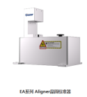
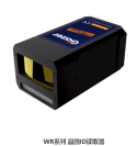
2) Core optical components for semiconductors
Components such as wafer calibrators, wafer ID readers, laser driver light sources, and batch wafer code readers act as the "nerve center" of the production line, providing highly stable underlying support for equipment and effectively reducing reliance on external suppliers. Leveraging its fully independent intellectual property rights, the company's products have obtained SEMI international certification and participate in the formulation of national standards for the semiconductor industry.

1765391345279.png

Please, Log in or Register to view URLs content!


tokenanalyst

Lieutenant General
Registered Member

Jingce Electronics secures a 433 million yuan order for semiconductor mass testing equipment.​

Jingce Electronics issued an announcement stating that its controlling subsidiary, Shanghai Jingce Semiconductor Technology Co., Ltd. (hereinafter referred to as "Shanghai Jingce"), and other subsidiaries within the company's consolidated scope signed multiple sales contracts with the same counterparty and its related companies within 12 consecutive months, with a total contract amount of approximately RMB 433 million.

The announcement shows that Jingsheng Electronics mainly sells semiconductor metrology equipment such as film thickness series products, OCD equipment, and electron beam equipment to customers. The main application scenarios are advanced memory and HBM-related fields.

1765403050873.png
1765403817888.png


Jingsheng Electronics stated that the signing of the contract reflects the customer's high recognition of the company's semiconductor metrology equipment, which will help expand the company's brand influence and enhance its market competitiveness. If this batch of contracts is successfully fulfilled, it is expected to have a positive impact on the company's operating results.

Please, Log in or Register to view URLs content!
 
Top