Chinese semiconductor industry

Status
Not open for further replies.

sunnymaxi

Captain
Registered Member

Huawei discloses patent for "wafer processing device and wafer processing method"​


Huawei Technologies Co., Ltd. has recently added several pieces of patent information, one of which is titled "Wafer processing device and wafer processing method" and the public number is CN117219552A.

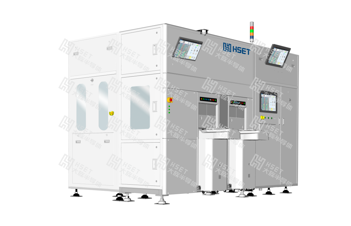
The patent abstract shows that embodiments of the present disclosure relate to wafer processing apparatuses and wafer processing methods. The wafer handling device includes: a wafer stage that can rotate along a rotation axis; a robotic arm, including a robot hand, for handling the wafer and placing the wafer on the wafer stage; a controller; and a calibration component , including: a grating plate, fixed relative to the wafer stage; a light source, fixed relative to the grating plate; and an imaging element, fixedly provided on the robotic arm, and adapted to receive light emitted from the light source and transmitted through the grating plate; wherein , the controller is configured to control the mechanical arm or the adjustment device on the mechanical arm to adjust the position of the wafer based on the detection of the received light by the imaging element; wherein, when the wafer stage carries the wafer, the grating plate The imaging element and the imaging element are respectively located on opposite sides of the plane where the upper surface of the wafer carrier is located, and the upper surface is used to carry the wafer. The devices and methods provided by embodiments of the present disclosure can improve wafer alignment efficiency and alignment accuracy.

It is reported that as of the end of 2022, Huawei holds more than 120,000 valid authorized patents, mainly distributed in China, Europe, America, Asia Pacific, the Middle East and Africa. Among them, Huawei holds more than 40,000 patents in China and Europe each, and more than 22,000 patents in the United States.

Please, Log in or Register to view URLs content!
 

sunnymaxi

Captain
Registered Member

Han’s Semiconductor: Committed to becoming a benchmark company in the field of semiconductor equipment manufacturing​


Han's Semiconductor mainly researches processing technologies applied to materials such as silicon, silicon carbide, gallium arsenide, gallium nitride, ceramics, sapphire, glass, flexible films and metals, and produces, manufactures and sells a series of automated processes from fine micromachining to visual inspection. Professional equipment.

Han's Semiconductor has undertaken the national "13th Five-Year Plan" - the key project of the National Ministry of Science and Technology's key R&D plan "Ultra-short pulse laser stealth cutting system and application"; the national "14th Five-Year Plan" - the key project of the National Ministry of Science and Technology's key R&D plan "High "Development and application demonstration of high-quality laser stripping and debonding equipment"; Shenzhen's key technology research and development project "High-precision proximity lithography equipment for 5G communications and new display fields", etc. This year, Han’s Semiconductor also passed the certification of “National High-tech Enterprise”.

Han's Semiconductor competes for the "Annual Outstanding Innovative Product Award" on the IC Billboard with its fully automatic laser grooving machine DSI-S-GV5242.
797533662563.2903.png


GV5242 is used in fields such as grooving and cutting of metal layers and special functional layers on wafer surfaces. Han's Semiconductor stated that this equipment breaks foreign monopoly and is the first domestic slotting equipment used in front-end yellow light workshops and is specifically used for 3D stacked advanced packaging. Different from ordinary 2.5D chip stacking, this technology uses new processes to integrate storage, logic, and sensors, which can further break through Moore's Law.

Han's Semiconductor competes for the "Annual Technology Breakthrough Award" in the IC Billboard with its fully automatic laser debonding equipment DSI-S-DB661.
1556473116879.727.png


Equipment DSI-S-DB661 is mainly used for temporary bonding of 12-inch (compatible with 6/8-inch) glass slides and wafers (thickness 50~3000μm) in integrated circuit inFO and 2.5D/3D advanced packaging processes under normal temperature conditions. The laser debonding and separation process is carried out, as well as the cleaning of Release carbon ash and residual bonding glue on the wafer after debonding. This equipment has been stably produced in Shenghe Jingwei, Changdian Shaoxing, Huajin Semiconductor, Huawei Technologies, Yuntian Semiconductor, Huatian Technology, China Ordnance, China Power 55 Institute and other companies. At the same time, it assists customers in packaging process research and development, and the cost is controllable. In this case, the density and speed of the Internet will be further improved.

Please, Log in or Register to view URLs content!
 

tokenanalyst

Brigadier
Registered Member

3.6 billion! The second phase of large funds invests in Huahong Chengdu​


According to industry news, the second phase of a large fund invested in Huahong Chengdu, a new company of the "unfinished" wafer factory Chengdu GlobalFoundries, with a subscribed investment of 3.6 billion yuan!

According to reports, Huahong Chengdu has recently completed its first capital increase since its establishment. The registered capital has increased from 100 million yuan to 22.8 billion yuan. Among them, the original sole shareholder and a member of the Huahong Group, Shanghai Huali Microelectronics Co., Ltd. The company (hereinafter referred to as "Huali Micro") subscribed to Huahong Chengdu's new registered capital of 11.6 billion yuan; Chengdu High-tech Lianxin Technology Industry Investment Co., Ltd. subscribed to 7.5 billion yuan; National Integrated Circuit Industry Investment Fund Phase II Co., Ltd. Then subscribed 3.6 billion yuan.

After the capital increase is completed, the three parties hold approximately 51.32%, 32.89% and 15.79% of Huahong Chengdu's registered capital respectively. At present, Huahong Chengdu's registered capital of 22.8 billion yuan has exceeded domestic wafer fabs such as Shanghai Huahong Grace Semiconductor Manufacturing Co., Ltd. and Semiconductor Manufacturing International Corporation (Shanghai) Co., Ltd.
It is understood that on the east side of the Chengdu High-tech Comprehensive Free Trade Zone, the GF project, which originally planned to invest nearly US$10 billion, has now been replaced by the logo of "Huahong Integrated Circuit (Chengdu) Co., Ltd." at the gate.​

Please, Log in or Register to view URLs content!
 

tokenanalyst

Brigadier
Registered Member

Zhongke Zhongyi's self-developed power gallium nitride on silicon production line is put into operation​


Zhongke Zhongyi Semiconductor Technology Co., Ltd., recently, Suzhou Zhongke Zhongyi Semiconductor Materials Co., Ltd. (hereinafter referred to as "Zhongke Zhongyi") independently developed large-size silicon-based gallium nitride for use in the field of power electronics. (GaN-on-Si) epitaxial wafer production line was officially built and put into use. This means that the production of power gallium nitride epitaxial wafers in the direction of power electronics will get rid of dependence on imports and become completely independent and controllable.

Relying on its advanced R&D and industrialization base, Zhongke Zhongyi focuses on the R&D and manufacturing of large-size silicon-based gallium nitride epitaxial wafers for third-generation semiconductors, and is committed to providing high-quality gallium nitride material solutions for the power electronics field. According to reports, the gallium nitride epitaxial wafer produced by Zhongke Zhongyi has a gallium nitride layer thickness of about 5 μm, no cracks on the surface, and a warpage of less than 100 μm. At room temperature, the HEMT structure has a sheet resistance of 465Ω/sq, a two-dimensional electron gas (2DEG) concentration of about 8×1013cm-2, a 2DEG mobility of greater than 2000 cm2/Vs, and intra-chip and inter-chip unevenness of less than 1%, which can meet The development and application needs of power devices in the field of power electronics have significantly reduced the production cost of gallium nitride epitaxial wafers while getting rid of dependence on imported equipment.

Please, Log in or Register to view URLs content!
 

tokenanalyst

Brigadier
Registered Member

This electronic specialty gas manufacturer plans an A-share IPO​


According to the official website, Yicu Gas was founded in 2006 and focuses on electronic special gases, electronic chemicals, electronic bulk gases, industry supporting special equipment, engineering, and operation and maintenance services. Through independent research and development and independent innovation, we will gradually implement a full range of domestic substitutions. The company has multiple business divisions. Through R&D centers, industrial bases, various sites and other models, the company has increased product categories and R&D investment, and comprehensively deployed in semiconductor, photovoltaic, panel, aerospace, pharmaceutical, precision chemistry and other industries.

Judging from the current equity structure, the controlling shareholder of Yicu Gas is Shanghai Yicu New Materials Group Co., Ltd., and the actual controllers are Li Jianxin and Zhu Yan. Among them, Shanghai Yicuo New Materials Group Co., Ltd. is a company in which Li Jianxin and Zhu Yan hold 100% of the shares. They directly hold 47.344% of the company's shares and are the company's controlling shareholders; Li Jianxin and Zhu Yan each directly hold 25.725% of the company's shares. % and 4.801% of the shares; Li Jianxin controls 1.589% of the company through Tianjin Henry Enterprise Management Partnership (Limited Partnership), Tianjin Henghui Enterprise Management Partnership (Limited Partnership), and Tianjin Henry Huirui Enterprise Management Partnership (Limited Partnership) respectively. , 1.047% and 0.795% of the shares. Therefore, Li Jianxin and Zhu Yan collectively control 81.301% of the company's shares and are the actual controllers of the company.​

1702565045383.png1702565077474.png

Please, Log in or Register to view URLs content!
 

tokenanalyst

Brigadier
Registered Member

The first wafer of Sany Shuozhou Phase II ultra-thin monocrystalline silicon wafer project comes off the production line​


Core tip: According to the official WeChat account of Shuozhou Municipal People’s Government, on December 9, the first silicon wafer of Sany Shuozhou Phase II ultra-thin monocrystalline silicon wafer project successfully rolled off the production line. A square rod of monocrystalline silicon with a length of about 830 mm has been passed through 100

According to the official WeChat account of Shuozhou Municipal People’s Government, on December 9, the first silicon wafer of Sany Shuozhou Phase II ultra-thin monocrystalline silicon wafer project successfully rolled off the production line. A square rod of about 830mm long monocrystalline silicon can be turned into 4,580 silicon wafers after more than 100 minutes of processing. The relevant person in charge said that all the main equipment for the project will arrive in early January next year, and the entire project will be put into production at the end of January. Based on industry needs, "Sany" Group will continue to increase investment and develop the photovoltaic manufacturing industry chain of "monocrystalline silicon - slices - solar cells - photovoltaic modules".


tphuang

Lieutenant General
Staff member
Super Moderator
VIP Professional
Registered Member
Please, Log in or Register to view URLs content!

Hangzhou Lion which is a foundry for RF/power chip (IIRC) among other things has 3 new projects

1 to produce 1.8m 12-inch Si wafers per year
second to produce 720k 6-inch power chip projects
third to produce 2.4m 6-inch wafer substrate
 

tokenanalyst

Brigadier
Registered Member

Xingxin and Peking University EDA Research Institute established a joint laboratory​

Peking University Electronic Design Automation Research Institute (Peking University EDA Research Institute) held an unveiling ceremony. Academician Huang Ru expressed congratulations on the unveiling of the institute via video, and more than 100 experts from the school and enterprises, including Academician Park Shilong, participated in the event.
At the unveiling ceremony, Dr. He Qing, chairman and CEO of Hangzhou Xingxin Technology Co., Ltd., and Professor Wang Runsheng, dean of the EDA Research Institute of Peking University, signed a contract to build a joint laboratory. Dr. He Qing said that the joint laboratory will focus on the field of EDA sign-off, leverage the respective advantages of Xingxin and Peking University, carry out in-depth cooperation in basic and applied research, talent training, etc., and jointly establish an EDA industry innovation ecosystem.

Xingxin-Peking University EDA Research Institute Joint Laboratory
The industry-education integration innovation laboratory jointly established by Xingxin and Peking University EDA Research Institute aims to develop cutting-edge theories and key technologies around key needs such as Signoff EDA technology, chip design methodology, high-performance computing, EDA industry standards, and talent training. joint innovation. The purpose of establishing the joint laboratory is to jointly build a scientific and technological innovation path with deep integration of industry, academia and research, and to strengthen the team of high-level EDA professional talents. By integrating the advantages of both parties, we can jointly overcome problems and transform the scientific research results of universities into actual market applications. Through continuous innovation, we can promote the construction of new materials, new processes, and new architecture advanced processes in the entire chain of integrated circuit design and EDA software, and promote major chip innovations. Application implementation promotion.

Please, Log in or Register to view URLs content!
 

tokenanalyst

Brigadier
Registered Member
Please, Log in or Register to view URLs content!

This company is working on thin-disk laser for next-generation LPP-EUV light source, which they claim to be the only viable laser type for next gen LPPEUV. Trumpf, the supplier of CO2 lasers for current generation LPP light source, is again the leading player in this new laser type.
CIOMP LPP laser will hit like 43 KW 100 KHZ next year but the advantage of this light source is the can be used as MHZ EUV FEL if scaled enough.

Please, Log in or Register to view URLs content!
 
Status
Not open for further replies.
Top