Chinese semiconductor industry

Status
Not open for further replies.

tokenanalyst

Brigadier
Registered Member
1702491486480.png

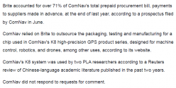
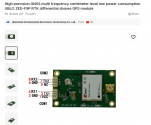
Do any of these mainstream journalists do even do the minimum research before writing stupid crap? These are CIVILIAN SPECS GNSS modules that you can find on Alibaba around 240 bucks a piece, for 200 bucks a piece they will deliver you 500 pieces right to your door ANYWHERE, INCLUDING TO THE 50 STATES OF UNITED STATES OF AMERICA.


1702491264336.png

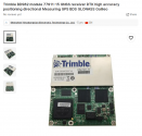
These "PLA researchers" may as well have bought Swiss made UBLOX modules for 150 bucks for 1000 pieces or better yet 50 industrial grade trimble GNSS modules for 1600 bucks a piece.
1702492482004.png1702492619121.png

This what happen when you let these know nothing Think Tankers take control of the narrative, because these US politicians are like 5 year olds, you have to explain them things little by little, they dont care about logic, nuance or the technical background behind the things they are legislating, they
only care about the narrative, in this case "China Bad".
 

european_guy

Junior Member
Registered Member
That would tell me de-americanized 14nm process should go into production sometimes middle of next year

Is it possible to increase 14nm and even 7nm capacity with 28nm localization?

I asked myself this question for a while, but I'm not from this industry so I don't have a clear answer.

I mean even lithography tools, that are the most bounded for a specific process node, can be used on a somewhat wide node range. For instance ASML 1980Di can be used for 28nm, but also at 14nm and IIRC TSMC used it for their first 7nm.

And this is lithography. For etching, deposition, etc.. AMAT / LAM and the Japanese they don't have 10 models, but at best just a couple of models for 28nm and below nodes.

So, in case these tools, are replaced with localized tool for 28nm, maybe they can be physically moved to a14nm line or even a 7nm line, increasing capacity at advanced nodes.

For instance a possible SMEE litho at 28nm, with AMEC NAURA and even Kingstone (ion implantation) can "free" a whole bunch of foreign tools that can be reused at 14nm or below.

This is a way to indirectly increase capacity at advanced nodes using new Chinese equipment at 28nm node.
 

theorlonator

Junior Member
Registered Member
Is it possible to increase 14nm and even 7nm capacity with 28nm localization?

I asked myself this question for a while, but I'm not from this industry so I don't have a clear answer.

I mean even lithography tools, that are the most bounded for a specific process node, can be used on a somewhat wide node range. For instance ASML 1980Di can be used for 28nm, but also at 14nm and IIRC TSMC used it for their first 7nm.

And this is lithography. For etching, deposition, etc.. AMAT / LAM and the Japanese they don't have 10 models, but at best just a couple of models for 28nm and below nodes.

So, in case these tools, are replaced with localized tool for 28nm, maybe they can be physically moved to a14nm line or even a 7nm line, increasing capacity at advanced nodes.

For instance a possible SMEE litho at 28nm, with AMEC NAURA and even Kingstone (ion implantation) can "free" a whole bunch of foreign tools that can be reused at 14nm or below.

This is a way to indirectly increase capacity at advanced nodes using new Chinese equipment at 28nm node.
Do AMAT and LAM really have that few models? Sounds like it shouldn't be super hard to adjust Chinese tools to higher nodes if they're just improvements on tools they already have.
 

sunnymaxi

Major
Registered Member
Is it possible to increase 14nm and even 7nm capacity with 28nm localization?

I asked myself this question for a while, but I'm not from this industry so I don't have a clear answer.

I mean even lithography tools, that are the most bounded for a specific process node, can be used on a somewhat wide node range. For instance ASML 1980Di can be used for 28nm, but also at 14nm and IIRC TSMC used it for their first 7nm.

And this is lithography. For etching, deposition, etc.. AMAT / LAM and the Japanese they don't have 10 models, but at best just a couple of models for 28nm and below nodes.

So, in case these tools, are replaced with localized tool for 28nm, maybe they can be physically moved to a14nm line or even a 7nm line, increasing capacity at advanced nodes.

For instance a possible SMEE litho at 28nm, with AMEC NAURA and even Kingstone (ion implantation) can "free" a whole bunch of foreign tools that can be reused at 14nm or below.

This is a way to indirectly increase capacity at advanced nodes using new Chinese equipment at 28nm node.
something interesting for you..

28nm tools will be same for 7nm or 5nm.jpg

company itself says, their 28nm tools can be used in 7nm process too.. i believe with little modification and upgradation 28nm tools can be used in 7nm process just like 1980i litho ..

the big thing is, China now have 28nm local supply chain. they just need to climb up for high end process.. maybe this is the reason why SMIC and Huawei is so confident as the releasing new products in the market ..
 

european_guy

Junior Member
Registered Member
Is it possible to increase 14nm and even 7nm capacity with 28nm localization?

I asked myself this question for a while, but I'm not from this industry so I don't have a clear answer.

I mean even lithography tools, that are the most bounded for a specific process node, can be used on a somewhat wide node range. For instance ASML 1980Di can be used for 28nm, but also at 14nm and IIRC TSMC used it for their first 7nm.

And this is lithography. For etching, deposition, etc.. AMAT / LAM and the Japanese they don't have 10 models, but at best just a couple of models for 28nm and below nodes.

So, in case these tools, are replaced with localized tool for 28nm, maybe they can be physically moved to a14nm line or even a 7nm line, increasing capacity at advanced nodes.

For instance a possible SMEE litho at 28nm, with AMEC NAURA and even Kingstone (ion implantation) can "free" a whole bunch of foreign tools that can be reused at 14nm or below.

This is a way to indirectly increase capacity at advanced nodes using new Chinese equipment at 28nm node.


EDIT: People correctly suggest to upgrade the Chinese 28nm tools to advanced nodes. This is the main / long term approach...but a more immediate one is to use foreign tools, currently installed on a 28nm line, for more advanced nodes.

The assumption here is that a brand new, just validated Chinese 28nm tool is not as mature and reliable (and maybe not as performant) as a foreign tool used also at 28nm, but already proved also at more advanced nodes.
 
Last edited:

tokenanalyst

Brigadier
Registered Member
Do AMAT and LAM really have that few models? Sounds like it shouldn't be super hard to adjust Chinese tools to higher nodes if they're just improvements on tools they already have.
LAM has 9 families of etching products and the flex family has like 7 products but I guess those are mainly upgrades "you know the benefit of working with fabs in a positive feedback cycle", Naura has 5 families and the biggest one the NMC has 8 products, AMEC has the Primo family divided on 9 etching products.

Just like AMEC and Naure not all families are used in Front-end fabrication or in advance process nodes.
 

sunnymaxi

Major
Registered Member
EDIT: People correctly suggests at this point to upgrade the Chinese 28nm tools to lower nodes. This is the main / long term approach...but a more immediate one is to use foreign tools at 28nm for lower nodes.

The assumption is that a brand new, just validated Chinese 28nm tool is not as mature and tested (and maybe not as performant) as a foreign tool used also at 28nm, but already proved also at more advanced nodes.
lower nodes ? you were talking about higher nodes using 28nm tools .. maybe typing error .. XD
 

tokenanalyst

Brigadier
Registered Member

Detection of carbon contamination in EUV multilayer mirrors based on secondary electrons.​


State Key Laboratory of Applied Optics, Key Laboratory of Optical System Advanced Manufacturing Technology,
Changchun Institute of Optics, Fine Mechanics and Physics, Chinese Academy of Sciences, Changchun.
University of Chinese Academy of Sciences, Beijing, 100039, China

Abstract​

The issue of carbon contamination on the surface of extreme ultraviolet (EUV) optical elements needs to be addressed urgently. In the process of removing carbon contamination, it is necessary to detect the thickness of the carbon contaminated layer in order to avoid damage to EUV multilayer mirrors (MLMs) by overcleaning. The yield of secondary electrons (SEY) generated by the excitation of EUV photons and primary electrons has been proved to be correlated with the thickness of the carbon layer, and thus the cutoff point for carbon layer cleaning can be found by detecting the SEY. In this study, the spatial distribution and motion state of secondary electrons (SEs) in the vacuum cavity of the EUV system during the cleaning process are described, utilizing the Particle-in-cell model and Monte Carlo method, and the variation relationship between SEY and the thickness of the carbon layer is obtained. The results show that under the set conditions, the SEY generated by EUV photons is very low, but it will generate primary electrons that are 1.05 times as numerous as itself, of which 24% bombarded to the carbon layer, resulting in SEs which amount to 16% of primary electrons generation. Moreover, as the carbon layer thickness decreases to 2 nm or below, SEY increases significantly, ranging from 0.55 to 0.71. The present work is of great significance in realizing the accurate detection of the carbon layer thickness of EUV multilayer film mirrors and the recovery of the reflectivity of MLMs.

Please, Log in or Register to view URLs content!
 
Status
Not open for further replies.
Top