Founded in 2018, Jiangling Technology is committed to providing high-end optical measurement and inspection equipment to global semiconductor customers, and strives to build Asia's first-class semiconductor quality inspection equipment company.
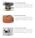
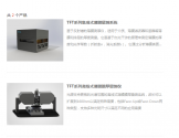
Jiangling Technology is headquartered in Lingang, Shanghai, with a R&D center in Zhangjiang, Shanghai, and a manufacturing base in Changshu, Jiangsu. Jiangling Technology integrates R&D, manufacturing and sales. Its core products include front-end critical film measurement equipment, front-end OCD measurement equipment, advanced packaging 3D and 2D inspection equipment, etc. Jiangling Technology focuses on independent research and development of core technologies, and has taken the lead in breaking through the technical difficulties of "key thin film measurement" and "Micro-Bump 3D measurement". Its core products have been recognized by mainstream wafer factories and advanced packaging factories at home and abroad. While establishing a good customer reputation, we continue to obtain bulk repeat purchases from customers.
As of mid-2023, Jiangling Technology has delivered more than 50 units of equipment that are in mass production, and some of the equipment has been exported to Europe, Southeast Asia and Taiwan. In the past three years, the number of customers of Jiangling Technology has grown rapidly, and the company's revenue has maintained an annual growth rate of more than 100%. Revenue in 2023 will exceed 50 million yuan, and orders on hand will exceed 100 million yuan. In the next two years, the company's order quantity and revenue will Revenue will maintain rapid growth.


