What phone app would take advantage of peak transfer rates asides from editing 8K videos or large dataset manipulation? 8500MB/ps RAM speed is overkill for 99.9% of use cases and difference is not even that large to be noticeable.8500MB/ps vs 9600
You are using an out of date browser. It may not display this or other websites correctly.
You should upgrade or use an alternative browser.
You should upgrade or use an alternative browser.
Chinese semiconductor industry
- Thread starter Hendrik_2000
- Start date
- Status
- Not open for further replies.
SMIC isWho produces these fancy desk top CPU chips that Loonsong designs?
another SMIC product. I don't know why this is so hard to figure out. Why it's sidestepping us sanctions.
A super computer using LA664 cores will be much better than this sunway core architecture
Sundak: Self-developed and launched AdaptStar high-end test machine to solve many technical problems.
Sundak is a global high-tech company specializing in semiconductor testing equipment technology research and development, production, sales, consulting and service. The company is headquartered in Shanghai and has offices in Suzhou, Xi'an, Shenzhen, Chengdu and other places.
Sundak passed ISO9001 certification in 2018, passed the high-tech enterprise certification in 2021, and became a "Specialized, Specialized, Specialized and New" enterprise in Shanghai in 2022. In the same year, it was successfully selected as a "Specialized, Specialized, Specialized and New" Little Giant Enterprise by the Ministry of Industry and Information Technology.
Sundak independently developed and launched the AdaptStar system integrated circuit high-end testing machine, which is mainly used to meet the needs of domestic and foreign semiconductor packaging and testing manufacturers for integrated circuit packaging testing and other mechanical automation production, thereby improving the production efficiency of semiconductor packaging and testing links and ensuring Semiconductor finished product quality and application effects. The company focuses on research and development and independent technological innovation. The products it develops and the services it provides provide customers in the industry with optimized semiconductor equipment solutions and successfully solve many technical problems.
They also manage to get cooperation agreement with the Shanghai Automotive Inspection Center for auto chip inspection.
Work together to build an innovation ecosystem for the automotive chip industry—Sundac & Shanghai Automotive Inspection signed a strategic cooperation agreement
In order to seize new strategic opportunities, build new development momentum, and help the high-quality development of the automotive chip industry, Sundak Semiconductor Technology (Shanghai) Co., Ltd. (hereinafter referred to as "Singdak") recently cooperated with Shanghai Motor Vehicle Inspection and Certification Technology Research Center Co., Ltd. (hereinafter referred to as "Shanghai Automotive Inspection") signed a strategic cooperation agreement. The two parties will give full play to their respective advantages and coordinate development in the field of automotive chips, and explore the formation of a result-oriented strategic cooperation model that meets the common development needs of both parties.
Geize Technology completed tens of millions of yuan in financing
Recently, GEZE Precision Technology (Suzhou) Co., Ltd. (hereinafter referred to as GEZE Technology) recently completed a new round of financing with a financing amount of tens of millions of yuan. This is the company's second successful round of financing this year.
This round of financing is a new round of financing after receiving tens of millions of yuan in Pre-A round strategic investment in May 2023 (Pre-A round financing was invested by Xiaomiao Fund and Su Gaoxin Science and Technology Angel Fund), and was funded by Su Venture Capital· Guofa Venture Capital, Su Gaoxin Rongsheng, Yuanhe Yuandian, Zehe Venture Capital, Zhuoyuan Capital and other institutions jointly invested. It is worth noting that Su Gaoxin’s investment in this round is also a renewal investment, which shows its high recognition of GEZE.
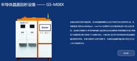
According to Gezer Technology CEO Zhou Yichu, Gezer Technology is a high-tech company engaged in semiconductor optical measurement equipment and industrial intelligent optical sensing products. Its semiconductor measurement equipment is mainly used for defect detection and parameter measurement in the semiconductor manufacturing process. It is widely used in wafer manufacturing, chip manufacturing, advanced packaging and other fields. With the development of advanced semiconductor processes, measurement equipment has ushered in a broad space for development; in the field of high-end smart sensors, GEZE Technology adheres to the internationally advanced product positioning, implements independent innovation, and leads cutting-edge technology research and development policies to industrialize and Engineering is the research goal, and the current advantages in high-performance optical sensors are used to serve the fields of high-end industrial manufacturing and intelligent industrial production. A variety of optical sensing products developed by the company have been widely used in high-end manufacturing fields such as lithium battery production and new energy manufacturing.
Gezer Technology’s current main focus is semiconductor front-end testing equipment. This field has long been monopolized by imported brands such as Onto innovation, Thermo Scientific, and Semilab. With the rise and progress of domestic high-end manufacturing, especially the urgency of localization in the semiconductor field, front-end measurement in the semiconductor production process has become very important. Once the measurement and measurement links are stuck, the entire industry will fall short. Since its establishment, GEZE Technology has achieved a series of breakthroughs in independent innovation. It has completed Online wafer measurement technology for 12-inch large-size wafers, covering FTIR film thickness measurement technology, element concentration measurement technology, etc., which can be applied to silicon, Many large and medium-sized domestic semiconductor companies have begun to use GEZE products in large quantities to meet the demand for mass inspection of silicon carbide, gallium nitride, gallium arsenide, indium phosphide and other material wafers.

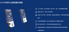
In the field of industrial automation, Gazer Technology has launched high-end intelligent sensing products such as high-precision edge measurement sensors, reflective edge measurement sensors, and high-precision groove sensors through independent innovation, which are widely used in lithium battery production, new energy manufacturing, and 3C. Production, health care and other fields, and has been applied in the production lines of well-known customers such as CATL.

I’m pretty sure Huawei has it's own fab,which makes their chips now. I'm not talking about the new fab being build in ShenZhen,which is still under construction.
Remember back in 2020-2021,there were reports on several domestic equipment and material supplier(I think I did post some on this thread),mentioned about Huawei as one of their customers. Only fabs need to buy those stuff.
There was a rumour on internet that Huawei modified some second hand lithography machine to improve the accuracy. This rumour alone doesn't sounds very credible,but about a year ago,there was a news that SMEE was complaining to Shanghai local official that Huawei was poaching their engineers. Why would any fab need to poach lithography machine design engineers,if they are just a regular lithography machine user?Only those with the intention of creating new,or modify existing lithography machine would do so.
they do have their own fabs as others have said here, but they are basically still on 28nm node and looking to solving 14nm. And they will try to produce a lot of the chips they need. Makes sense for them and othersI’m pretty sure Huawei has it's own fab,which makes their chips now. I'm not talking about the new fab being build in ShenZhen,which is still under construction.
Remember back in 2020-2021,there were reports on several domestic equipment and material supplier(I think I did post some on this thread),mentioned about Huawei as one of their customers. Only fabs need to buy those stuff.
There was a rumour on internet that Huawei modified some second hand lithography machine to improve the accuracy. This rumour alone doesn't sounds very credible,but about a year ago,there was a news that SMEE was complaining to Shanghai local official that Huawei was poaching their engineers. Why would any fab need to poach lithography machine design engineers,if they are just a regular lithography machine user?Only those with the intention of creating new,or modify existing lithography machine would do so.
Bro I agree with most of your statement except that SMEE is an integrator, maybe my opinion, Huawei is doing the same thing and may compete with SMEE as there is a need to fast track the introduction of front end lithography as urgency dictate. They are the end user and have experience working with TSMC and now with SMIC, so they know what is needed to quicken it's introduction.I’m pretty sure Huawei has it's own fab,which makes their chips now. I'm not talking about the new fab being build in ShenZhen,which is still under construction.
Remember back in 2020-2021,there were reports on several domestic equipment and material supplier(I think I did post some on this thread),mentioned about Huawei as one of their customers. Only fabs need to buy those stuff.
There was a rumour on internet that Huawei modified some second hand lithography machine to improve the accuracy. This rumour alone doesn't sounds very credible,but about a year ago,there was a news that SMEE was complaining to Shanghai local official that Huawei was poaching their engineers. Why would any fab need to poach lithography machine design engineers,if they are just a regular lithography machine user?Only those with the intention of creating new,or modify existing lithography machine would do so.
- Status
- Not open for further replies.
