Chinese semiconductor industry

Status
Not open for further replies.

tokenanalyst

Brigadier
Registered Member

Urupu successfully launches wafer resistivity measurement equipment SICV200​

Urupa Semiconductor Equipment (Wuxi) Co., Ltd. ("Urupup" for short) announced that the company has recently successfully launched the wafer resistivity measurement equipment SICV200 and will soon be delivered to customers for verification.

1701094782780.png


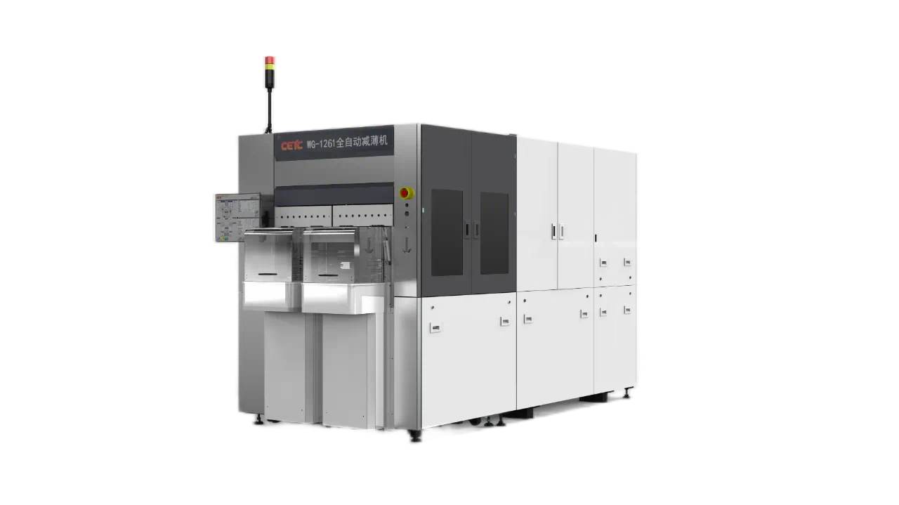
SICV200 is a semiconductor measurement equipment used to measure the resistivity of silicon wafers and the doping concentration of silicon carbide or other semiconductor materials. It can support sustained multi-frequency CV on wafers of various sizes including 12 inches. Characterization analysis. In terms of machine configuration, SICV200 has semi-automatic solutions of various sizes and fully automatic solutions that comply with SEMI standards. It can be directly connected to the MES system of the customer's factory to achieve automated production.

1701094822576.png
Dr. Tang Deming, general manager of URP, said that carrier concentration is an important technical parameter when performing homoepitaxial growth on a substrate. Currently, the industry generally uses the capacitance voltage (CV) method to measure the carrier concentration of the homoepitaxial layer. This method can directly form a Schottky barrier on the semiconductor to measure the carrier concentration of the epitaxial layer, and can also form a MOS capacitor structure to monitor the CVD process, thereby effectively evaluating the carrier concentration of the epitaxial layer in various semiconductor material manufacturing processes. The carrier concentration and the quality of the epitaxial layer can be measured and analyzed conveniently and non-destructively to provide basis and support for optimizing the epitaxial growth process.

1701094874943.png

In terms of technical solutions, Urupu has made corresponding improvements and optimizations to the equipment in response to the suggestions and pain points put forward by customers during use, fully considering the independent controllability of the supply chain and domestic substitution needs, and has made progress in intellectual property rights and innovation.

Previously, Urupu has launched the first domestic semiconductor-specific FTIR (Fourier Transform Infrared Spectroscopy) measurement equipment:
  • Suitable for silicon-based epitaxial layer thickness measurement equipment Eos200/Eos300
  • Applicable to silicon-based element concentration (B/P/F) measuring equipment Eos200+/Eos300+
  • Through optimized hardware design (updated infrared spectrometer technology) and self-developed algorithms, the Eos200L, a device for measuring the film thickness of silicon carbide (SiC) epitaxial layer and epitaxial buffer layer, is realized.

Please, Log in or Register to view URLs content!
 

sunnymaxi

Captain
Registered Member

Beijing CETC: 100% independent research and development, WG-1261 fully automatic thinning machine has entered the mass production stage​


WG-1261 fully automatic thinning machine is a fully automatic thinning machine suitable for mass production of 6-8 inch SiC substrates and wafers. It was independently developed by Beijing Zhongdian Technology and has obtained 5 authorized patents.

This fully automatic thinning machine is equipped with a high-power and high-torque spindle, which can achieve high efficiency, high precision, and damage-free mirror processing. The dual-spindle and three-station design ensures processing efficiency, and is equipped with a real-time online measurement unit (measuring range 0-1800μm) , precise control of thinning thickness; equipped with SECS/GEM networking function. In addition, it is equipped with SMIF (optional) to maintain high cleanliness while performing stable thinning grinding..

1279417799820.0364.png


The WG-1261 fully automatic thinning machine mainly has three key technologies and innovations: a high-power low-vibration air-floating spindle suitable for grinding hard and brittle materials and a high-rigidity and high-precision air-floating stage. It is 100% independently developed and suitable for carbonization. Silicon material thinning and grinding; high-rigidity and low-vibration air-floating rotary system realizes high-precision, low-vibration smooth switching of wafers between rough grinding, fine grinding, and loading and unloading stations; wafer thickness automatic adjustment system realizes micron Level automatic adjustment, compatible with anti-vibration stability, meeting grinding process requirements.

At present, the WG-1261 fully automatic thinning machine is mainly used in 6- and 8-inch silicon carbide substrates and silicon carbide devices. It has cooperated with leading silicon carbide substrate companies Tianke Heda, Shuoke Crystal, Shandong Tianyue, etc. , the equipment has entered the mass production stage, all technical indicators meet customer requirements, and the on-site use results are good. In addition, we have also cooperated with China Electronics 13th Institute, Zhejiang Xinke, China Electronics 55th Institute, etc. in terms of silicon carbide devices. Now the equipment has entered the mass production stage and the processing data meets the requirements.

Looking forward to the future, Beijing CETC will continue to provide domestic and foreign customers with higher-quality thinning machines, dicing machines and other equipment, making new contributions to the development of my country's integrated circuit industry.

Please, Log in or Register to view URLs content!
 

measuredingabens

Junior Member
Registered Member
Seven fabs seems excessive. Just to manufacture what a couple million cars. I guess they are trying to get as much money from different municipalities which is why they are doing it like this. Typically concentrating production in semis leads to increased savings with scale.
Which is why for example TSMC used to operate like it did with megafabs and be quite successful. TI is also basically getting rid of its 200mm fabs and moving to all 300mm fabs. TI is going to use 300mm even for old processes with legacy chips. Which is going to give them a competitive advantage due to lower manufacturing cost per chip.

Of course you might still use smaller diameter wafers for discretes like transistors and on things which don't use silicon.

Is there any information on these fabs? Like process and capacity?
Isn't BYD also a supplier for phonemakers as well? As phonemakers increasingly localise their suppliers, it seems prudent for BYD to expand in that area.
 

tokenanalyst

Brigadier
Registered Member


Silan Micro: Plans to raise 4.96 billion yuan, and National Fund will participate in the second phase of subscription​


Silan Micro disclosed a report on the issuance of stocks to specific targets on the evening of November 22. It plans to issue 248 million company shares, raising a total of 4.960 billion yuan and a net amount of approximately 4.913 billion yuan.

The announcement shows that the funds raised from this private increase will be used for the annual production of 360,000 pieces of 12-inch chip production line projects, SiC power device production line construction projects, automotive semiconductor packaging projects (Phase I) and to supplement working capital. Silan Micro said that the implementation of this fundraising project will help the company further increase the production capacity and sales proportion of emerging products such as automotive-grade power modules, promote the upgrading and transformation of product structure; help the company form a pioneer in the field of power semiconductors development advantages, scale advantages and cost advantages, thereby enhancing customer service capabilities and market competitiveness, and continuing to consolidate the company's dominant position as a leading domestic semiconductor IDM enterprise; it will help the company improve its industry voice and international influence, and help the company build a world-class The strategic development goal of becoming a competitive comprehensive semiconductor product supplier.

It is worth noting that the company's related party National Integrated Circuit Industry Investment Fund Phase II Co., Ltd. (referred to as "Big Fund Phase II") participated in the subscription of stocks issued to specific objects this time, and its planned subscription amount is 1.24 billion yuan.

Please, Log in or Register to view URLs content!
 

tokenanalyst

Brigadier
Registered Member

Fast diffraction model of an EUV mask based on asymmetric patch data fitting.​


Calculating the diffraction near field (DNF) of a three-dimensional (3D) mask is a key problem in the extreme ultraviolet (EUV) lithography imaging modeling. This paper proposes a fast DNF model of an EUV mask based on the asymmetric patch data fitting method. Due to the asymmetric imaging characteristics of the EUV lithography system, a DNF library is built up including the training mask patches posed in different orientations and their rigorous DNF results. These training patches include some representative local mask features such as the convex corners, concave corners, and edge segments in four directions. Then, a convolution-based compact model is developed to rapidly simulate the DNFs of 3D masks, where the convolution kernels are inversely calculated to fit all of the training data. Finally, the proposed model is verified by simulation experiments. Compared to a state-of-the-art EUV mask model based on machine learning, the proposed method can further reduce the computation time by 60%–70% and roughly obtain the same simulation accuracy.

Please, Log in or Register to view URLs content!
 

tphuang

Lieutenant General
Staff member
Super Moderator
VIP Professional
Registered Member
Please, Log in or Register to view URLs content!

Gigadevice and its GD32F4 series MCU has joined Xiaomi Vela IoT ecosystem and is integrated with it.

Demonstrated GD32F470I-EVAL development kit for the purpose of building new products with it and verifying functions

Looks like about 20+ ecosystem partners in there
 

luminary

Senior Member
Registered Member
Disappointed, I'd have liked to see the full shadow ban on exports kept. We've gone over this, halfassing restrictions is counterproductive.

Please, Log in or Register to view URLs content!

After almost zero exports were recorded in August and September, tiny quantities were posted for October, according to the latest Chinese customs data. For germanium, exports were 0.65 tons, compared to 8.78 tons in July. For gallium, they were 0.25 tons, versus 7.58 tons in July.
 
Status
Not open for further replies.
Top