Chinese semiconductor industry

Status
Not open for further replies.

antiterror13

Brigadier
Please, Log in or Register to view URLs content!

very interesting to look at Sunway (shenwei)'s new super computer use SW26010-Pro processors. It's now officially the 2nd fastest super computer in the world. Although who knows what unreported super computers in china have.

Seems like they just packed in an absurd amount of cores in here to get the high computation
But it seems not in the official list
Please, Log in or Register to view URLs content!
 

tokenanalyst

Brigadier
Registered Member

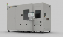
Yaoguang semiconductor laser annealing equipment successfully passed the acceptance inspection!​

Recently, Yaoguang's semiconductor laser annealing equipment has been debugged and verified by the customer's new production line and confirmed to meet mass production requirements. The yield exceeded expectations and successfully passed the acceptance inspection!
This equipment has been put into production in the customer's new production line. The production line plans to produce 100 million power chips and 10,000 6-inch SiC epitaxial wafers annually , including "100,000 silicon carbide epitaxial wafers and JBS and MOSFET power integrated circuits." " .
1700921442283.png
The SiC/Si-based laser annealing equipment independently developed by Yaoguang Semiconductor is widely used in multiple processes such as silicon-based IGBT ion doping activation and silicon carbide back electrode coating annealing. Its microsecond-level control system, wafer thickness measurement function and excellent optical shaping device provide an efficient solution for the wafer annealing process.

This equipment acceptance marks that the "Yaoguang Semiconductor Laser Annealing Project" has passed the last milestone (PP valve point) of the development process ESDP. From the perspective of equipment industrialization, the effectiveness and reliability of the ESDP forward development process are further verified. At the same time, it also provides a reliable R&D theoretical basis for the forward development of new projects such as Yaoguang Semiconductor's MOCVD and RTP rapid annealing. In the future, the company will continue to increase investment in research and development to help achieve my country's goal of "overtaking around the corner" in the semiconductor industry.​

Please, Log in or Register to view URLs content!
 

tokenanalyst

Brigadier
Registered Member

China Electronics Technology (Shanxi) Third Generation Semiconductor Technology Innovation Center project main body capped​


Walking into the project construction site, material transport trucks shuttled in an orderly manner, and curved-arm self-propelled lift trucks moved up and down along the wall. As the operator's instructions were issued, the large crane waved its arms to steadily transport the huge rock wool sandwich panels to the designated location. “Since construction started on August 12 this year, the East District A05 third-generation semiconductor technology innovation center test verification center with a construction area of 17,000 square meters and the A10 comprehensive warehouse with a construction area of 5,000 square meters were completed in just over three months. For the construction of the main structure, the installation of the metal enclosure structure on the wall and the spraying of internal fireproof coatings have begun." The on-site construction leader of Eleven Technology, the construction unit, introduced that the project department, on the premise of doing a good job in safe production, based on the actual winter construction conditions , provide logistical support for more than 100 workers working hard at the construction site in the east and west districts, and equip outdoor workers with cold-proof equipment to ensure the smooth progress of the project.

China Electronics Technology (Shanxi) Third Generation Semiconductor Technology Innovation Center is located in Xiaohe Emerging Industrial Park, Shanxi Comprehensive Reform Demonstration Zone, and is implemented by China Electronics Technology Second Institute. Including the third-generation semiconductor technology innovation center test verification line and supporting projects covering an area of 203 acres in the east district, and the microelectronics intelligent manufacturing industry base project covering an area of 312 acres in the west district. The total planned investment is 1.27 billion yuan and will be constructed in two phases. After the completion of the first phase of the project, it will have the ability to produce 600 units/set of intelligent manufacturing equipment and 24,000 pieces/year of ceramic substrates and circuit modules. It will also build a 6-inch wide bandgap semiconductor manufacturing equipment process verification platform and a common technology research and development platform.

Please, Log in or Register to view URLs content!
 

tokenanalyst

Brigadier
Registered Member

Changdian Technology’s advanced packaging solutions for high-precision millimeter wave radar meet the diverse needs of customers​

.
As the world's leading chip manufacturing service provider, Changdian Technology has created complete advanced millimeter wave radar packaging solutions and accumulated rich mass production experience to meet the diverse needs of customers in various fields such as autonomous driving, intelligent transportation, and smart homes. need.
Millimeter-wave radar has become a popular technology in many intelligent application fields in recent years due to its advantages such as small size, easy integration, high spatial resolution, and strong anti-interference ability, and has broad market prospects. Guosen Securities predicts that the global millimeter wave radar market will reach 38.4 billion yuan by 2025, with a compound growth rate of 25.5% from 2021 to 2025.
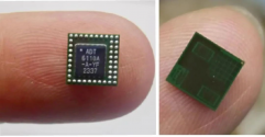
The hardware core of millimeter wave radar includes MMIC and antenna. The system architecture consists of antenna, transceiver module, power management, signal processing and other parts. Chip packaging methods mostly use flip-chip packaging, fan-out packaging, and AiP (Antenna in Package) packaging that integrates antenna and radar transceiver chips.
In the high-precision millimeter-wave radar market, Changdian Technology cooperates with many leading millimeter-wave radar chip customers at home and abroad to develop, using packaging technologies such as eWLB and FC flip-chip to meet the needs of customer products with multiple transceiver channels, integrated antennas, and low power. consumption needs and help customers enrich their product lines. At present, Changdian Technology has achieved large-scale mass production of millimeter wave radar products.
The industry's leading millimeter-wave radar chip provider Aanda Technology has maintained a long-term cooperation with Changdian Technology to provide the market with millimeter-wave radar solutions that are easy to integrate, low energy consumption and highly cost-effective. Based on Antenna Technology's CMOS millimeter wave radar SoC chip, the newly launched 60GHz AiP (Antenna in Package) and 77GHz AiP series of millimeter wave radar chips further reduce the complexity and cost of millimeter wave radar systems. During the cooperation process, Changdian Technology has provided complete flip-chip (FCCSP) integrated antenna AiP and other packaging products in view of the multi-scenario application characteristics of the product, achieving small size, high yield, high reliability and low cost of the product, which can meet the needs of Application needs in multiple fields such as automotive intelligent driving, intelligent cockpits, smart homes, drones, and intelligent transportation.
1701033396668.png

Please, Log in or Register to view URLs content!
 

tphuang

Lieutenant General
Staff member
Super Moderator
VIP Professional
Registered Member

so this is interesting to look at just how much more expensive the Western chip options are vs Horizon and SemiDrive chips.

Both new companies using just A5x series cores in their SoC. Low cost and the chips are cheap too.

The cockpit SoC by Unisoc, Rockchip and SiEngine all have combination of A76 and A55 cores (all about same in performance and cost).

But you see with increased funding the horizon chip now look far more impressive in computation power (they are using 14 A78AE core CPU on J6). Ideally as SemiDrive has more money and backers, it can go develop higher performing chips also. That's basically the idea of success breeding success.

Only when Chinese startups achieve success and find customers can they be more ambitious on their next projects
 

gelgoog

Lieutenant General
Registered Member
IMHO these companies are making a mistake with their lineup. It would be much better just to make chips with only ARM Cortex A-510 cores. The Cortex A-510 is 64-bit and comes with minimal baggage for backwards compatibility with 32-bits. You can also use a merged core where you have two cores use the same floating point unit together.
 

tphuang

Lieutenant General
Staff member
Super Moderator
VIP Professional
Registered Member
They developed those chips using what was available and cheap at the time of development. A510 may not have fit those conditions. Now that they have more money, let's see if they can develop more advanced chips.

Anyways, BYD semi development. Developed their own audio amplifying chip and they have actually quite a few fabs around the country now. Latest one to open is in Shaoxing.


gelgoog

Lieutenant General
Registered Member
Anyways, BYD semi development. Developed their own audio amplifying chip and they have actually quite a few fabs around the country now. Latest one to open is in Shaoxing.
Seven fabs seems excessive. Just to manufacture what a couple million cars. I guess they are trying to get as much money from different municipalities which is why they are doing it like this. Typically concentrating production in semis leads to increased savings with scale.
Which is why for example TSMC used to operate like it did with megafabs and be quite successful. TI is also basically getting rid of its 200mm fabs and moving to all 300mm fabs. TI is going to use 300mm even for old processes with legacy chips. Which is going to give them a competitive advantage due to lower manufacturing cost per chip.

Of course you might still use smaller diameter wafers for discretes like transistors and on things which don't use silicon.

Is there any information on these fabs? Like process and capacity?
 

tokenanalyst

Brigadier
Registered Member

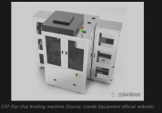
Liande Equipment: The die bonding machine used in the advanced packaging field has been delivered for mass production​


Liande Equipment stated on the investor interaction platform on November 27 that the company is actively deploying in the semiconductor field and has successfully entered the semiconductor packaging and testing industry with the successful development of semiconductor IC packaging equipment. At present, eutectic, soft solder and other die bonding machines and equipment such as QFN lead frame coating and lead frame inspection have been delivered to customers for mass production. The company will actively create and seize development opportunities in the field of semiconductor equipment, accelerate technology research and development and market development in the field of semiconductor equipment, and strive to achieve rapid business development.

Liande's die-bonding machine equipment can be used in the field of advanced packaging, mainly semiconductor die-bonding machines, including display driver chip COF flip-chip machines, semiconductor flip-chip machines, soft solder die-bonding machines, eutectic die-bonding machines, etc.

1701094623135.png

Please, Log in or Register to view URLs content!
 
Status
Not open for further replies.
Top