Unless the companies themselves, whether SME, designers, foundries, etc publish it straight from their own sources everything anyone says, whether its from people closer to the industry or observers is still an educated estimate or guess, although some may be closer to the truth then others. Since this is facts/evidence based forum, without statements from the source of truth (the companies themselves) basically everything we say here is a presentation/debate of best guesses/opinions based on observed details. I think it is fair to ask/challenge someone to provide a reasoning/basis for what they stand behind, and @hvpc and other industry experts such have more then provided their rationale for where they stands. Others are free to disagree with this conclusion, and vice versa. It is unfair to rag/attack on him as if he is downplaying progress or denigrating the work being done. I personally think its great to see an inside perspective, helps me learn and put so many things into perspective and I wouldn't want to lose a perspective just because its not as optimistic. We shouldn't let this turn into a positive-reinforcement circle jerk like some others we won't name so lets judge progress and achievements by the results, such as published statements/product output/deliveries from the industry participants and then we can award a medal to who is closest to the truth.you know what guys.....I'm a bit tired of thankless effort to share my insights.
I think it'll make your lives and mine a lot simpler if I don't stir the pot with info I'm privy to. i'll let you guys go back to scavenging for info from the media.
You are using an out of date browser. It may not display this or other websites correctly.
You should upgrade or use an alternative browser.
You should upgrade or use an alternative browser.
Chinese semiconductor industry
- Thread starter Hendrik_2000
- Start date
- Status
- Not open for further replies.
Systematical Investigation of Flicker Noise in 14 nm FinFET Devices towards Stochastic Computing Application
1- State Key Laboratory of Fabrication Technologies for Integrated Circuits, Institute of Microelectronics of the Chinese Academy of Sciences, Beijing 100029, China2-School of Microelectronics, University of Chinese Academy of Sciences (UCAS), Beijing 101408, China
3-School of Microelectronics, University of Science and Technology of China, Hefei 230026, China
4-College of Communication Engineering (College of Microelectronics), Chengdu University of Information Technology, Chengdu 610225, China
Abstract
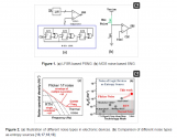
Stochastic computing (SC) is widely known for its high error tolerance and efficient computing ability of complex functions with remarkably simple logic gates. The noise of electronic devices is widely used to be the entropy source due to its randomness. Compared with thermal noise and random telegraph noise (RTN), flicker noise is favored by researchers because of its high noise density. Meanwhile, unlike using RRAM, PCRAM and other emerging memory devices as the entropy source, using logic devices does not require any additional process steps, which is significant for industrialization. In this work, we systematically and statistically studied the 1/f noise characteristics of 14 nm FinFET, and found that miniaturizing the channel area of the device or lowering the ambient temperature can effectively increase the 1/f noise density of the device. This is of great importance to improve the accuracy of the SC system and simplify the complexity of the stochastic number generator (SNG) circuit. At the same time, these rules of 1/f noise characteristics in FinFET devices can provide good guidance for our device selection in circuit design.

2. Device Fabrication and Experiments
The FinFET devices are fabricated based on the Semiconductor Manufacturing International Corporation (SMIC) 14 nm FinFET CMOS process platform. The Fin width (Tfin) and height (Hfin) were 12 nm and 21 nm, respectively, and the effective device width was approximately given by Nfinger × Nfin × (2 × Hfin + Tfin). So, the channel area of the FinFET device is calculated as follows:Here, A is the channel area, Weff is the effective device width, and L is the channel length
It is unfair to rag/attack on him as if he is downplaying progress or denigrating the work being done. I personally think its great to see an inside perspective, helps me learn and put so many things into perspective and I wouldn't want to lose a perspective just because its not as optimistic.
Downplaying, uplaying, pessimistic, optimistic doesn't matter, asking someone for sources as far I understand is not denigrating them. I think to the contrary providing sources will only enrich this thread. Or at least the information should be distilled in a way that make logic sense without giving too much if the person wants. IDK.
If we are going that route, a insider in Shanghai told me that that Huawei and SMIC are making 7-5nm chips in high volume using a shinny Free Electron Laser EUV machine. Sources? I don't want to stir the pot.
If we are going that route, a insider in Shanghai told me that that Huawei and SMIC are making 7-5nm chips in high volume using a shinny Free Electron Laser EUV machine. Sources? I don't want to stir the pot.
Well according to electronics weekly YMTC was outputting 200K wafers per month in their fab2 facility last year, that is between their 128L and 232L products, I could assume that they could be outputting around 50K wpm of 232L NAND in just that facility.
Not to put a damper on the enthusiasm, that article is from August 2022 before the October restrictions.
Wow, that is unbelievable. They are using Newsonic N40/N41 BAW filters for 5G. Something i would not have expected at all.
Samsung Galaxy Tab A9 entry level tablet teardown,lots of Chinese components inside
Lansus 2G PA
Radrocktech 4G PA
Newsonictech BAW and SAW filter
Radrocktech switch
Maxscend switch
Awinic LNA
View attachment 121708
View attachment 121701
View attachment 121702
View attachment 121703
interesting that they mention ODM Huaqin's help here in getting the Chinese RF chips into Galaxy, but obviously the companies themselves still have to be competitive
Keep in mind these Newsonic filters are for N40/41 band, so still doesn't seem to have anything for the 77 to 79 band which occupies the higher frequency range
Looks like SMEC has been fabbing their RF filter for a while. I just still haven't seen the higher band stuff新声半导体在中芯宁波代工的体声波滤波器良率和可靠性快速提升。已经支持多家设计公司实现射频前端中高频BAW滤波器量产。
Give it to two years. TI will see significant declines in China. I don't think people on this forum realize just how much Chinese auto industry for example relies on TI chips at the moment or how that is going to change
And not just in MCU but also Analog space
On this one, from April's Shanghai auto show
看完这届车展,芯片的竞争局势更加明了:国产芯片公司地平线、黑芝麻智能、芯驰、辉羲智能等组队,围攻英伟达、TI、Mobileye等国外芯片玩家。主要有两块战场:
- 大算力芯片:以地平线J5、黑芝麻A1000,去和英伟达Orin竞争;
- 低算力芯片,以地平线J3、芯驰V9P,去和TI的TDA4竞争
现在,TI的TDA4成了更多国内车企的选择。
哪吒S、岚图Free搭载的均是TDA4芯片。另据HiEV了解,这届车展上最新发布的岚图追光,采用的是双TDA4芯片。
so because TI's TDA4 became the first obvious one in the market, it had a lot of domestic market share. But as these other local players like SemiDrive, Horizon, Cambrian & black sesame have come on the market, there is not really much advantage in various TDA4 products但提到拼成本,国产芯片公司更为擅长,地平线J3、黑芝麻智能A1000 L、芯驰V9P正在蚕食TI TDA4的市场。地平线J3最为活跃。
低算力芯片市场,还杀出了芯驰科技、寒武纪这样的黑马。芯驰推出的智能驾驶芯片V9P,AI算力为20TOPS,基于单芯片可以实现AEB、ACC、LKA等功能和辅助泊车、记忆泊车功能,且可以集成行车记录仪和高清360环视。
寒武纪推出SD5223,面向L2+自动驾驶行泊一体,16TOPS 算力,支持8M IFC、5V5R、10V10R三种产品形态,其中5V5R 方案单颗SOC实现行泊一体功能,并可采用自然散热,推动自动驾驶系统向10-15万元的入门级车型覆盖
主要以地平线J3、芯驰V9P、TI TDA4为主,采用5V5R的主流方案,瞄准20万元以下车型。中低端市场,地平线J3、芯驰V9P打的是TDA4mid;
中端市场,黑芝麻智能A1000打的是TDA4VH;
By the way, this applies to other SoC and MCUs also from NXP like S32G and Renesas in V3H
All chips that are not that high end in computation. Should be not too difficult to replace
so if firms like Horizon are willing to work closely with automakers to fully utilize their chips, no wonder they get chosen至于TI,在软件方案支持上,也不像国内芯片玩家那样提供全面服务。“要在TI(TDA4) 的芯片上做软件方案是有难度的。某种程度上,这也是地平线的J3和J5扩展迅速的一个重要原因。” 行业媒体从业者宇多田援引一位技术大佬的话表示,“地平线保姆式做法,就是芯片上自搭了感知,特别是J2和J3。”保姆式的做法,芯片公司称为参考算法。车展期间,地平线副总裁兼软件平台产品线总裁余轶南向HiEV在内的媒体透露,“地平线去年已经向客户开放了一套BEV的参考算法。我们现在是完全支持占用网络的,未来在合适时间会围绕包括占用网络这样的算法向合作伙伴分享。”
More importantly, as a single chip is able to do the central ADAS control in the future, you really only need just 1 SoC to do all the handling. Eventually, you will be able to get all you need for both smart cockpit and ADAS.
And if you can do it for something complicated like EVs, then other things should be easy
Wow, that is unbelievable. They are using Newsonic N40/N41 BAW filters for 5G. Something i would not have expected at all.
interesting that they mention ODM Huaqin's help here in getting the Chinese RF chips into Galaxy, but obviously the companies themselves still have to be competitive
Keep in mind these Newsonic filters are for N40/41 band, so still doesn't seem to have anything for the 77 to 79 band which occupies the higher frequency range
Wait a minute,newsonictech has no N40/41 band filters,not according to their website

you know what guys.....I'm a bit tired of thankless effort to share my insights.
I think it'll make your lives and mine a lot simpler if I don't stir the pot with info I'm privy to. i'll let you guys go back to scavenging for info from the media.
I appreciate them even if I don't always agree. I wouldn't take opposition to your comments too seriously. It's an unfortunate but inevitable outcome of any large public forum. You get a lot of commentary regardless of how unqualified it is.
I think b40 and b41 are for n40/n41Wait a minute,newsonictech has no N40/41 band filters,not according to their website
View attachment 121716
- Status
- Not open for further replies.


