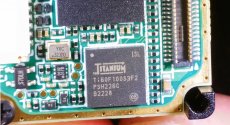
These teardown shows that,even for WIFI chips,advanced node is important,28nm is not good enough,you need at least 14nm for advanced WIFI chips
You are using an out of date browser. It may not display this or other websites correctly.
You should upgrade or use an alternative browser.
You should upgrade or use an alternative browser.
Chinese semiconductor industry
- Thread starter Hendrik_2000
- Start date
- Status
- Not open for further replies.
I tried to collect some info regarding this coating/developing process that IMHO is a bit underestimated. It is a critical process where currently Japan has a dominant position.
I'm not an expert here, so I thank in advance if knowledgeable people in the forum correct / improve the text.
1. Cleaning: prerequisite step, but not part of coating/developing
Vapor primer oven
2. Dehydration bake 150 °C for ten minutes
3. Vapor primer deposition of adhesion promoter HMDS
This step lays down a thin layer of HMDS (HexaMethylDiSilazane) that allows the resist to have a better adhesion to the substrate
Performing the dehydration bake and vapor prime in the same oven gives optimum performance.
Coater
4. Spin coating the bottom antireflective coating (BARC)
5. Hot plate softbake to remove solvent
Another layer is added with an antireflective material that dumps the reflection of the lithography light when hits the wafer surface and is reflected back, so to avoid various issues like standing waves, etc. Needed for advanced nodes.
Coater
6. Spin coating the photoresist
7. Hot plate softbake to remove solvent
With a different machine, but of the same type (coater), the resist is finally applied by spin coating. After this, inside the same machine, wafer is baked to dry it and evaporate the excess solvent. Hot plate is currently the most common way to heat the wafer.
8. Lithographic Exposure by e.g. ASML machine
Developer
9. Hot plate post-exposure bake (PEB) for CA resists
10. Spray development with TMAH (Tetramethylammonium hydroxide) on spin equipment
11. Rinse with de-ionized water and dry with nitrogen flow
12. Hot plate + UV postbake to harden the resist image
My understanding is that all the above can occur in a single machine (developer).
Post-exposure bake is needed for chemically amplified resist to finalize the chemical reaction in the resist, started with the light exposure. While postbake curing is used to hardening the already developed resist to better sustain the following etching process.
Plasma asher (used as descummer)
13. Photoresist plasma descum to remove the residual photoresist
After development, some minimal trace of photo-resist can still be found in in the open trenches or holes, this step, removes a very thin layer of resist across the wafer, removing the resist residual.
It's amazing to me how many processes (13) are actually needed for a single lithography step.
Last edited:
I think there is a big difference between FinFET and other process. If you watch their chip design, Hisilicon really utilizes SMIC 14nm for anything that doesn't have highest level of space/power constraintThese teardown shows that,even for WIFI chips,advanced node is important,28nm is not good enough,you need at least 14nm for advanced WIFI chips
HiSilicon Hi1105GFCV120 Wi-Fi 6/BT 5.2/SparkLink SoC Floorplan Analysis (IoTB)
This is a Basic Floorplan Analysis (BFR) of the HiSilicon Hi1105GFCV120_die found inside HiSilicon Hi1105GFCV120. The Hi1105GFCV120 was extracted from the Huawei Mate 60 Pro. The Hi1105GFCV120 die is fabricated using a two-layer passivation, ten layers of metal interconnect (one aluminum (Al) top metal layer and nine copper (Cu) layers), tungsten (W) contacts, shallow trench isolation (STI), a single polysilicon layer, and high-k metal gate (HKMG) finFET transistors. The observed minimum metal pitch contacted gate pitch and fin pitch are 68 nm, 96.0 nm and 48 nm, respectively. These critical dimensions, along with the observed features of the transistors, suggest that the Hi1105GFCV120 die was manufactured on 300 mm wafers using SMIC's 14 nm HKMG finFET process.
Broadcom BCM4398 Wi-Fi 7/BT 5.2 Combo SoC Floorplan Analysis (IoTB)
This report is a Basic Floorplan Analysis (BFR) of the Broadcom BCM4398 die found inside the Universal Scientific Industrial G5-602550 component. The BCM4398 die was manufactured on 300 mm wafers using TSMC's 7 nm HKMG finFET CMOS process. It features 17 metal interconnect layers (1 aluminum (Al) top layer, 16 copper (Cu) layers). The minimum observed metal, contacted gate, and fin pitches of 40 nm, 57 nm, and 30 nm, respectively.
Which means even as they swap 14nm for 7nm production at SMSC, getting more 14nm capacity using domestic tools is just as critical.
Also, it shows that Huawei is reasonably confident about SMSC capacity level if it's getting so deep into chip design again. You see Hisilicon SoC in so many more IoT devices now. You can only do that if you are confident about supply chain
big moment for China' AI inference chips
Horizon has now come out with Journey 6 SoC
Each chip supports 24 camera/Lidar/other sensors. Can handle full aspect NOA including all city driving scenarios
Customers include BYD, GAC, Bosch, Li Auto & VW/Cariad
560 TOPS & 350K DMIPS computation using BPU 3.0 (new generation AI processing)
Horizon has now come out with Journey 6 SoC
Each chip supports 24 camera/Lidar/other sensors. Can handle full aspect NOA including all city driving scenarios
Customers include BYD, GAC, Bosch, Li Auto & VW/Cariad
560 TOPS & 350K DMIPS computation using BPU 3.0 (new generation AI processing)
Investment exceeds 2.8 billion! Xinhua Semiconductor polysilicon project to be completed by the end of the month
A major project in the autonomous region—Inner Mongolia Xinhua Semiconductor Technology Co., Ltd.’s 10,000-ton semiconductor-grade polysilicon project was completed at the end of November.

At the construction site of Inner Mongolia Xinhua's 10,000-ton electronic-grade polysilicon project, there are many tower cranes, transportation vehicles shuttle back and forth, and more than 1,700 workers are stepping up construction. At the end of November, the entire project will be completed and single-machine debugging will be carried out.Li Mingfeng, executive deputy general manager of Inner Mongolia Xinhua Semiconductor Technology Co., Ltd.: "The investment in this project is about 2.8 billion, the output value is about 2.4 billion, and it can produce 10,000 tons of electronic-grade polysilicon."In recent years, Hohhot City has seized the autonomous region's major opportunities to promote high-quality development of new energy and new materials industries and created a large number of silicon material production, processing and manufacturing enterprises led by Zhonghuan Photovoltaics. This year, the construction of the Central Industrial City was launched, and a number of chain extension, chain reinforcement, and chain chain strengthening projects will be implemented. Inner Mongolia Xinhua Semiconductor Technology Co., Ltd.'s 10,000-ton semiconductor-grade polysilicon project is an important link in the industrial chain of Zhonghuan Industrial City.Wang Seal, Production Director of Inner Mongolia Xinhua Semiconductor Technology Co., Ltd.: "Xinhua is currently the largest semiconductor polysilicon supplier in China. After Inner Mongolia Xinhua is put into production, it will further expand its domestic market share advantage based on Jiangsu Xuzhou Xinhua .”
CETC Nanjing Epitaxial Materials Industrial Base Successfully Tried Production
Recently, China Electronics Semiconductor Materials Co., Ltd.’s Nanjing epitaxial materials industry base project announced that it has successfully completed trial production, taking an important step for the third-generation semiconductor materials industry. The industrial base is located in the Comprehensive Bonded Zone of Nanjing Jiangning Development Zone, covering an area of 100,000 square meters. The contract was signed on September 27, 2021.
The Nanjing epitaxial materials industry base project will be implemented in two phases, with an investment of up to 1.93 billion yuan in the first phase, focusing on the construction of third-generation compound epitaxial materials and 8-12-inch silicon epitaxial materials industrial bases. After the project is completed, it will create a production capacity of 4.56 million 8-12-inch silicon epitaxial wafers/year and 126,000 6-8-inch compound epitaxial wafers/year.
This important project achieved the rollout of the first silicon epitaxy and silicon carbide epitaxy in November 2022, marking that the industrial base has entered the trial production and verification stage. The project took just over a year from contract signing to trial production, demonstrating excellent progress speed.
The third generation of semiconductor materials, represented by silicon carbide and gallium nitride, has attracted much attention due to its advantages such as wide bandgap, high electron saturation drift velocity, high thermal conductivity, and large breakdown field strength. Silicon carbide power devices have broad application prospects in new energy vehicles, photovoltaics, rail transit, big data and other fields, while gallium nitride radio frequency devices have demonstrated high frequency, high power and wider bandwidth in 5G communications, Internet of Things, military radar and other fields. With the advantages of low power consumption.
In processing and preparation, the preparation of high-quality epitaxial materials on the substrate is considered to be the key to promoting the industrial application of third-generation semiconductors, and plays a key role in improving device performance and reliability. The successful trial production of CETC's Nanjing Epitaxial Materials Industrial Base marks a key step for the base in promoting the development of the third-generation semiconductor industry.
- Status
- Not open for further replies.


