Chinese semiconductor industry

Status
Not open for further replies.

hvpc

Junior Member
Registered Member
SMIC's N+2 process is supposed to have 113.6 million transistors per sq millimeter. This is basically the same as TSMC's N7+ using EUV in critical layers with 113.9 MTr/mm2. Compare that with when TSMC was still only using DUV. DUV only N7 process had 91.2 MTr/mm2.
SMIC's N+2 is slightly better in terms of density than Samsung's 6LPP process which has 112.79 MTr/mm2. It also compares much favorably in terms of density with Intel 7 which only has 100.76 MTr/mm2.

SMIC's N+2 is basically on the 6 nm intermediate node class in terms of transistor density. You could argue that in terms of transistor density SMIC is right now ahead of Intel until the Intel 4 process enters the market.

HiSilicon used the SMIC N+2 process in the Kirin 9000S. But they also used their own core design with two-way SMT. This means each core has higher multi-threaded performance than competing ARM core designs in the same process. This enables the processor to be competitive against 5 nm designs.
Your had made two mistakes:
TSMC 7nm+ basic cell size is 171x240nm
SMIC N+2 is 180x252nm. so your claim that N+2 share the same transistor density with TSMC 7nm+ is incorrect. If you use Apple-to-Apple calculation of assuming 60% NAND cell and 40% SFF cells, N+2 would have transistor density of about 103MTx/mma^2

(and if you use TechInsight's CPP measurement off the Kirin9000s, which is 63nm, instead of 60nm (which is what I used), then N+2 would have cell size of 189x252nm with corresponding transistor density of 98.1 MTx/mm^2).

Intel 10nm density is 100.76MTx/mm^2. The improved and newly named Intel7 has smaller cell size so has density of around 106MTx/mm^2.
 
Last edited:

BoraTas

Major
Registered Member
there's a few process node breakpoints where process chemistry changes such as poly-Si gate metal to metal gate conductor, oxide gate dielectric to high-k gate dielectric, going from planar to finFET, etc.
High-k was a huge thing when I started when 45 nm was about to get introduced. Then, if I remember correctly, fabs delayed the introduction which made everyone upset because we were having problems with power use at 45 nm.
 

tokenanalyst

Brigadier
Registered Member
HPO TM platform system realizes the ultimate DTCO - chip manufacturing from art to science to intelligence

The essence of design and manufacturing collaborative optimization (DTCO) is to achieve collaboration between design and manufacturing and allow each other's respective advantages to seek the overall optimal result. Different from traditional methods, the HPO TM proposed by Dongfang Jingyuan Microelectronics Technology (Beijing ) Co., Ltd. aims to establish a platform system and core engine around design, manufacturing and inspection to achieve real-time two-way data exchange in the design and manufacturing process. Ultimately, an integrated yield solution for collaborative optimization of design and manufacturing is realized so that the design department can obtain accurate and timely information to complete design iterations. At the same time, the chip manufacturing department can systematically consider the designer's intentions and ultimately achieve improvements in overall yield and efficiency. In this report, Dr. Yu will introduce the latest progress of Oriental Crystal Source and its affiliated companies in EDA tools such as layout and wiring, computational lithography (OPC), and defect detection analysis tools, demonstrating the HPO TM of Oriental Crystal Source after 10 years of efforts . How does the platform provide the industry with a more competitive integrated design and manufacturing yield solution in the post-Moore era.

Please, Log in or Register to view URLs content!
 

tokenanalyst

Brigadier
Registered Member

A key engineering project in Shanxi Province, Haina Semiconductor's silicon monocrystalline project is about to be put into production​


"Taiyuan Daily" reported on November 7 that the construction of the semiconductor silicon monocrystalline production base project of Haina Semiconductor (Shanxi) Co., Ltd. is nearing completion, and it is currently sprinting to put into production with all its strength.
Haina Semiconductor (Shanxi) Co., Ltd.'s semiconductor silicon monocrystalline production base project has a total investment of 546 million yuan, covering an area of approximately 133.85 acres and a construction area of approximately 89,700 square meters. The project uses Haina's own technology to introduce 120 sets of monocrystalline production equipment, build a 6-inch semiconductor silicon monocrystalline production base with an annual output of 750 tons, and carry out research and development of production technologies related to 8-inch to 12-inch semiconductor-grade silicon monocrystalline.
According to public information, Haina Semiconductor’s silicon monocrystalline production base project has been included in the key engineering projects of Shanxi Province.
Zhejiang Haina Semiconductor Co., Ltd. was established in September 2002. Its predecessor was the Zhejiang University Semiconductor Factory established in 1970. In September 2021, the company invested in Shanxi and established Haina Semiconductor (Shanxi) Co., Ltd. In January of the following year, Shanxi Haina Semiconductor's silicon monocrystalline production base project was settled in Yangqu Park. In May 2022, the project will start; in June 2023, the main factory building of the project will be capped.

Please, Log in or Register to view URLs content!
 

tokenanalyst

Brigadier
Registered Member

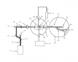
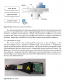
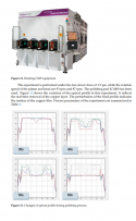
Endpoint Detection Based on Optical Method in Chemical Mechanical Polishing​


State Key Laboratory of Tribology, Tsinghua University, Beijing 100084, China

Abstract​

Endpoint detection is an important technology in chemical mechanical polishing (CMP), which is used to capture the material interface and compensate the variations of consumables and incoming wafer thickness. This paper aimed to apply optical detection in metal CMP. An in situ optical measurement system was developed for a 12-inch CMP tool. Kinematic analysis of the scanning trajectory of the laser device indicated the relative position relationship between the device and the wafer. Average optical data within the wafer described the material removal of metal CMP. Furthermore, optical data and location described the non-uniformity of the entire wafer surface. In this research, the polishing condition and the residual of the wafer edge are characterized by optical trace. Pauta Criterion is used to discriminate the inflexion point of the material interface. The results reveal that the interface capture is accurate and effective.

1699904114942.png1699904221747.png

Please, Log in or Register to view URLs content!
 

tokenanalyst

Brigadier
Registered Member

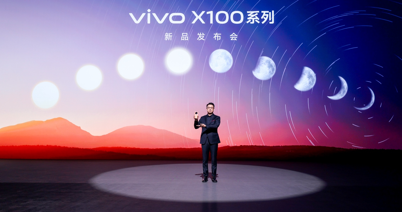
vivo releases vivo X100 series, AI large model mobile phone, equipped with 6nm self-developed imaging chip​

November 13, the vivo X100 series was released in Beijing. The vivo X100 series includes two models, X100 and X100 Pro, both of which use a new generation of self-developed imaging chips, higher standard optical lens modules and Dimensity 9300 ; The 7 billion parameter large language model on the terminal side and the 13 billion parameter model on the terminal side make the X100 series an AI large model mobile phone, priced from 3,999 yuan.
650805503815.6713.png

At the press conference, Huang Tao, vice president of vivo’s product line, introduced vivo’s technology brand “Blue Technology”. He said: "From X1 to X100, each generation of X series products has breakthroughs and innovations. Continuous super-saturated investment has allowed vivo to accumulate strong energy. Blue technology is the cornerstone of the core competitiveness of vivo products and the leading product experience Source, in the future, vivo will firmly continue to delve into the underlying technology and make Blue Technology more and more powerful."
The vivo X100 series fully covers core application scenarios through device-side deployment and cloud services of large-parameter AI computing power. The Lanxin Xiao V smart assistant function provides five experiences: super semantic search, super Q&A, super writing, super image creation, and super-sensory smart interaction, making the X100 series smarter.
The blue crystal chip technology stack promotes collaborative research and development in the industry chain through in-depth research on the underlying chip technology, combined with vivo's self-developed imaging chip capabilities, and brings a more powerful performance experience with integrated software and hardware design. The Blue Ocean battery life system takes a multi-pronged approach to create battery technology with larger capacity, faster flash charging, and thinner and lighter size. It also creates a new model of open source, consumption reduction, and efficiency improvement to meet users' new needs for mobile phone battery life. Blue River's self-developed operating system creates an Internet of Everything ecosystem for the AI era, with features that are smarter, smoother, and safer.
The vivo X100 series brings substantial upgrades in optics, computing power, and algorithms through the new Zeiss optical photography system, a fully upgraded set of computational photography supported by the 6nm self-developed imaging chip V3, a new super-sensing portrait system, and original image engine algorithms. Let the X100 series bring a better imaging experience in telephoto, portrait, night scene, video and other scenes.
 

tphuang

Lieutenant General
Staff member
Super Moderator
VIP Professional
Registered Member
Please, Log in or Register to view URLs content!

ChipOn's auto grade MCU KF32A158 recently passed ASIL-B safety grade certiication

In China's auto supplier show
Please, Log in or Register to view URLs content!
This new MCU has been award 荣获铃轩奖

Since passing ASIL-B auto grade, ChipOn has received interest from many automakers and tier-1 suppliers covering wheelbase, BCM & smart cockpit
 
Status
Not open for further replies.
Top