Chinese semiconductor industry

Status
Not open for further replies.

tokenanalyst

Brigadier
Registered Member

Jiyi Technology completed hundreds of millions of yuan in strategic financing, and Huatai United Securities served as the exclusive financial advisor to continue to empower the domestic semiconductor industry!


Recently, Shanghai Jiyi Technology Co., Ltd. (hereinafter referred to as "Jiyi Technology") announced the completion of hundreds of millions of yuan in strategic financing. This round of financing was funded by Tuojing Technology, Hefei Industrial Investment, Shengshi Capital, Jinding Capital, Fengyuan Capital, and Jingkai Capital, Yintai Huaying, Yixin Investment, Shanghai Renyi and other well-known institutions in the industry jointly invested, and Huatai United Securities served as the exclusive financial advisor. Previously, Jiyi Technology has introduced investments from many well-known institutions such as SMIC Juyuan, Yuanhe Puhua, Dachen Financial Intelligence, Haiwang Capital, Lingang Venture Capital, Jucheng Investment, Yangtze River Guohong and other well-known institutions.

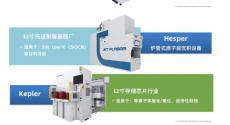
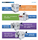
Jiyi Technology was established in 2015. It is a semiconductor equipment company focusing on the application of plasma and thermal deposition technology. It provides the industry with overall solutions for plasma and furnace tube applications. It is mainly used in compound semiconductor manufacturing, silicon-based semiconductor manufacturing, and semiconductor manufacturing. packaging, LED chips and other fields. The company builds process equipment for the full integrated circuit industry around plasma and thermal deposition technology. The core equipment covers plasma ashing equipment, plasma etching equipment, plasma nitriding equipment, atomic layering equipment, plasma processing systems, etc.

The core team members of Jiyi Technology are all from leading companies in the semiconductor industry at home and abroad. They have profound industry accumulation and have all-round industry competitiveness in technology research and development, application, sales and customer technical support. At present, the company's equipment surpasses leading overseas companies in many aspects of performance and process, and has entered leading companies in traditional chip packaging, LED chips, advanced chip packaging, compound semiconductor manufacturing, silicon-based semiconductor manufacturing and other fields, and has received a large number of orders. , breaking the monopoly of overseas manufacturers.

Yang Ping, chairman of Jiyi Technology, said that since the establishment of Jiyi Technology, the team has always insisted on working steadily and has gained recognition from leading customers in many product segments. This financing can receive investment from well-known industrial and financial investment institutions in the industry, which is a full recognition of Jiyi's technological products, technology, market and other capabilities. After this financing, Jiyi Technology will give full play to the business synergy of industrial capital, further increase investment in research and development, expand product layout, expand customer network and attract outstanding talents to join. In the future, Jiyi Technology will continue to devote itself to the research and development of semiconductor equipment and strive to become a leading company in the semiconductor equipment industry.

Xu Ding, head of investment at Tuojing Technology, said that Jiyi Technology is a very distinctive semiconductor equipment supplier in China and has strong synergy with the product line of Tuojing Technology. This investment by Tuojing Technology will further promote the cooperation between both parties. Collaborative development, we look forward to the two parties being able to deepen all-round cooperation in areas such as supply chain and market expansion in the future. We are firmly optimistic about and will continue to support the company's future development.

Looks like the launched new products.
1699807705328.png1699807790104.png

Please, Log in or Register to view URLs content!
 

tphuang

Lieutenant General
Staff member
Super Moderator
VIP Professional
Registered Member
interesting commentary by one of the more accurate weibo posters. Earlier, she said 7nm process had 117-120mmtr. Looks like a little back tracking here
SMIC N7 110mtr,N5预计135-140mtr,可以对比一下
someone likely passed this info to her. Likely she understands that it's internally identified as N+2, N+3, N+4, but maybe in a couple of years, they are expecting 135mmtr to be in production.
 

tokenanalyst

Brigadier
Registered Member

Baiwei Storage Huizhou Advanced Packaging and Testing Manufacturing Center Passed IATF16949 Automotive Industry Quality Management System Certification​


Shenzhen Baiwei Storage Technology Co., Ltd. ("Baiwei Storage" for short) focuses on the research and development, packaging, testing and manufacturing of memory chips. It is a national high-tech enterprise, a national-level specialized special new small giant enterprise, and has received strategic investment from the national large fund. The company closely focuses on the semiconductor memory industry chain and has built a business model integrating R&D, packaging and testing. It has core competitiveness in storage media characteristics research, firmware algorithm development, memory chip packaging and testing, test R&D, global brand operations, etc., and is actively Lay out chip IC design, advanced packaging and testing, chip testing equipment research and development and other technical fields.
In 2018, Baiwei Storage has passed the IATF16949:2016 automotive quality management system certification , reflecting the company's comprehensive strength in standardized management, quality control and technological innovation. Recently, Huizhou Baiwei, the advanced packaging and testing manufacturing center of Baiwei Storage, also successfully passed the IATF16949:2016 automotive industry quality management system certification. Huizhou Baiwei is positioned in advanced packaging and testing, has automotive-grade chip packaging and testing capabilities, and supports the parent company's automotive-grade chip business and its own automotive-grade packaging and testing foundry business. Passing the IATF16949:2016 certification this time is of great significance for the company to implement an intelligent management system, build automotive-grade quality control and process capabilities, and provide customers with high-quality products and services.

Please, Log in or Register to view URLs content!
 

tokenanalyst

Brigadier
Registered Member

With a total investment of 2 billion yuan, Wuxi Huishan has signed a new semiconductor core equipment project​


According to Jiwei.com news, on November 12, a semiconductor core equipment project with a total investment of 2 billion yuan was officially signed and implemented in Huishan District, Wuxi. In the future, a semiconductor core equipment production base will be built in Huishan High-tech Zone (Preparation) (Luoshe Town).

Image source: Released by Huishan High-tech Zone
According to news released by Huishan High-tech Zone, the project company will cooperate with Huishan High-tech Zone (in preparation) and Huishan Science and Technology Innovation Group to build a semiconductor core equipment project. The initial land will be 40 acres and a planned investment of 2 billion yuan will be formed in the future. "R&D in Shanghai" ", the main production base is in Wuxi" development pattern. After the Wuxi project is completed and reaches production, the annual output value is expected to exceed 700 million yuan. The person in charge of the project company said that the company was established in 2014 and focuses on the research, development and production of semiconductor technology equipment. At present, in addition to carrying out related equipment remanufacturing business, it also has the ability to self-research new equipment, and some self-developed products have been shipped.
 

Weaasel

Senior Member
Registered Member
Isn't that the view what alot of people in China,or even members on this very forum holds?How many times I heard something like “We don't need EUV,28nm is enough” “advanced node is too expensive,no one is going to buy that” “99% of semiconductor market is mature node,there is very little need for advanced node” etc.

I get it,because China cannot make advanced node now,so people will naturally dismiss the importance of advanced node,in order comfort themself,it's a psychological defence
That is no longer the attitude of most of the decision makers in China that matter...
 

european_guy

Junior Member
Registered Member

China Microchip releases a number of self-developed EDA tools to accelerate the construction of the entire process of domestic digital EDA​


Please, Log in or Register to view URLs content!

Dr. Bai Geng mentioned that after 2018, a large number of start-up companies have emerged in the domestic EDA industry, which has now increased from a dozen to over a hundred. Judging from the IC design tool chain, domestic EDA companies have basically covered every point tool. Although some tools have not yet reached commercialization standards, all covered point tools have been deployed and developed. Therefore, China's EDA industry has completed its development from 0 to 1

In 2022, it successfully released 14 EDA tools in five major series of Xintiancheng. It has now been promoted and implemented in many domestic chip design manufacturers and wafer fabs. use

China's EDA industry also needs to integrate through continuous mergers and acquisitions, and eventually form two or three leading companies and grow into a true full-process EDA tool integrator.

BTW this China Microchip company is GWX Shenzhen Guoweixin Technology 国微集团
Please, Log in or Register to view URLs content!


...Shenzhen?...wait, which other company is from Shenzhen?
 

Proton

Junior Member
Registered Member
Isn't that the view what alot of people in China,or even members on this very forum holds?How many times I heard something like “We don't need EUV,28nm is enough” “advanced node is too expensive,no one is going to buy that” “99% of semiconductor market is mature node,there is very little need for advanced node” etc.

I get it,because China cannot make advanced node now,so people will naturally dismiss the importance of advanced node,in order comfort themself,it's a psychological defence
I think it's the exact opposite: The notion that a good DUV scanner would effectively break the embargo has greatly increased with the release of Kirin9000s, proving that a less advanced node can make it in the premium space.
 
Last edited:

gelgoog

Lieutenant General
Registered Member
I think it's the exact opposite: The notion that a good DUV scanner would effectively break the embargo has greatly increased with the release of Kirin9000s, proving that a less advanced node can make it in the premium space.
SMIC's N+2 process is supposed to have 113.6 million transistors per sq millimeter. This is basically the same as TSMC's N7+ using EUV in critical layers with 113.9 MTr/mm2. Compare that with when TSMC was still only using DUV. DUV only N7 process had 91.2 MTr/mm2.
SMIC's N+2 is slightly better in terms of density than Samsung's 6LPP process which has 112.79 MTr/mm2. It also compares much favorably in terms of density with Intel 7 which only has 100.76 MTr/mm2.

SMIC's N+2 is basically on the 6 nm intermediate node class in terms of transistor density. You could argue that in terms of transistor density SMIC is right now ahead of Intel until the Intel 4 process enters the market.

HiSilicon used the SMIC N+2 process in the Kirin 9000S. But they also used their own core design with two-way SMT. This means each core has higher multi-threaded performance than competing ARM core designs in the same process. This enables the processor to be competitive against 5 nm designs.
 

tokenanalyst

Brigadier
Registered Member

Shengmei Shanghai (ACM Research Shanghai): Track equipment is expected to be connected with lithography machines by the end of the year, which will break the current market dominance of one company​


Shengmei Shanghai disclosed the latest research minutes saying that the company’s Track equipment has made good progress and is expected to be connected to the lithography machine by the end of this year. The biggest feature of the equipment is that it adopts advanced structural design and has the characteristics of high speed and high output. The current company's equipment can produce an output of 300-330 pieces, and in the future our architecture can also meet the output requirements of 400-450 pieces. At the same time, after more than ten years of accumulation, the company also has outstanding characteristics in terms of electronic control and software stability. In the future, we hope that the company's products can break the current monopoly in the market and allow the company to become the second supplier of Track equipment worldwide.

From the perspective of each product line, AMC Shanghai PECVD equipment team is actively cooperating with customers and has made considerable progress in software and hardware improvements. The company has taken a differentiated technical route for PECVD equipment and has its own patented IP, which also brings more technical parameters and performance exploration. Once the difficulties are completely overcome and verification and development is completed, the differentiated technology will bring huge output. In the future, the company's PECVD equipment will be introduced to the global market.

The company's electroplating equipment is relatively comprehensive. All types of electroplating equipment currently sold in the international market, including Damascus electroplating, TSV electroplating, advanced packaging electroplating, and third-generation semiconductor electroplating equipment, have been developed by the company, and have also been technologically advanced. verify. It is precisely because of its breakthroughs in electroplating that the company has received more repeat orders, which is also clearly reflected in revenue. It is expected that the company's electroplating products will continue to maintain rapid growth next year.

Shengmei Shanghai said that currently, the electroplating market is in a stage of rapid expansion, mainly due to the construction of front-end process plants and the demand for electroplating for 3D packaging, so we are very optimistic about the prospects of the electroplating market in the future. In the future, the company's electroplating equipment will also enter the international market, thereby benefiting from the growth of the global market.

Please, Log in or Register to view URLs content!
 
Status
Not open for further replies.
Top