Chinese semiconductor industry

Status
Not open for further replies.

tokenanalyst

Brigadier
Registered Member

Xinyuan Microsco completed industrial and commercial changes and added special equipment manufacturing for semiconductor devices, etc.​

Xinyuan Micro (KingSemi) announced that the company’s wholly-owned subsidiary Shanghai Xinyuan Micro Enterprise Development Co., Ltd. registered capital increased from RMB 300 million to RMB 520 million, an increase of 73.33%.

The business scope was changed from: sales of special equipment for semiconductor devices, sales of special electronic equipment, research and development of special electronic materials, engineering management services, etc., to: manufacturing of special electronic equipment, sales of special electronic equipment, manufacturing of special equipment for semiconductor devices , sales of special equipment for semiconductor devices, Electronic special materials research and development, mechanical parts / parts processing , mechanical parts / parts sales , engineering management services, etc.

Please, Log in or Register to view URLs content!
 

european_guy

Junior Member
Registered Member
The technology behind HBM is not difficult. But with the current DRAM capability of CXMT, stacking those chips may give you HBM2 level capability. But I don't see any point in using CPU/GPU that's a few generations behind (~1/3 the transistor density) along with HBM that's also a few generations behind (~1/4 the bandwidth & I/O speed) to come up with domestic GPU alternatives to compete against Nvidia. The gap will only continue to grow if we are stuck at N+2 & 18nm DRAM.

I'm really not an expert here, so please assume this is a question more then a statement.

I've checked pin transfer rates for different HBM and LPDDR generations, I assume pin transfer rate is the most critical enabler for each DRAM generation.

So
Please, Log in or Register to view URLs content!
standard allows for 2.4 Gbps per pin,
Please, Log in or Register to view URLs content!
formally tops out at 3.2Gbps/pin and HBM3 at 6.4Gbps/pin

Interestingly this is also the speed of
Please, Log in or Register to view URLs content!
, so it seems that from the technology point of view HBM3 is at the same level of LPDDR5.

According to CXMT roadmap, posted here few days ago, it seems CXMT is now testing/validating a LPDDR5 solution that plans to market starting Q2 2024.


cxm.jpg

So I wouldn't be so surprised if CXMT comes out with a HBM3-level product during 2024....of course it would be a huge thing anyhow.

Another point regarding HBM memory and AI chips in general, is that the required volumes are not as big as for general smartphones / CPU applications. So the day it will be needed, IMHO CXMT could cover this hole for China.
 

tphuang

Lieutenant General
Staff member
Super Moderator
VIP Professional
Registered Member
Please, Log in or Register to view URLs content!

Can we assume SMIC made also? Huawei & Loongson,
Of course, but loongson new chip uses 12nm process

Also I think when it comes to cxmt, they clearly need to be producing lpddr5 and getting into hbm. They will get there even if slower than we all want to see.
 

tokenanalyst

Brigadier
Registered Member
Is more than adding more transistors, a good architectural design can deliver a good performance than just dimensional scaling.

-----------------
Let’s start with a bit of a background. In a
Please, Log in or Register to view URLs content!
presented at the 2017 IEEE S3S conference, titled “A 1,000x Improvement in Computer Systems by Bridging the Processor-Memory Gap,” we introduced the potential of using hybrid bonding to overcome the “Memory Wall.” We further elaborated on this concept in a
Please, Log in or Register to view URLs content!
, titled “A 1000× Improvement of the Processor-Memory Gap,” published in the book NANO-CHIPS 2030,published in 2020.

On June 15, 2022, a Chinese
Please, Log in or Register to view URLs content!
titled “Breakthrough Bypassing the EUV Lithography Machine to Realize the Independent Development of DRAM Chips” reported that Xinmeng Technology had announced the development of a 3D 4F² DRAM architecture based on its HITOC technology. The company claimed that this architecture could be used as an alternative to advanced commercial DRAM. According to the article, this development represents another major innovation breakthrough in the field of heterogeneous integration technology, following the release of SUNRISE, an all-in-one AI chip for storage and computing. The article also reported that Haowei Technology had successfully used Xinmeng’s HITOC technology for the latest tape-out of the Cuckoo 2 chip, resulting in a large-capacity storage-computing integrated 3D architecture.

Techinsights is currently promoting a
Please, Log in or Register to view URLs content!
titled “China breaks through restrictions with advanced chiplet strategy: 3D-IC Breakthrough in Chinese Ethereum Miner.” According to the report, Techinsights discovered a storage mining design in the Jasminer X4 Ethereum miner ASIC, which was developed by the China-based manufacturer Jasminer. The report states that this design is the industry’s first-ever use of DBI hybrid bonding technology with DRAM. Techinsights highlights that the Jasminer X4 demonstrates how a Chinese company can combine mature technologies to creatively produce high-performance, cutting-edge applications even under trade restrictions. The report also reveals that the X4 features a sizable 32 mm × 21 mm logic die that employs the earlier XMC (Wuhan Xinxin Semiconductor Manufacturing Co.) planar 40/45 nm CMOS.

Please, Log in or Register to view URLs content!
 

tokenanalyst

Brigadier
Registered Member
Techinsights is currently promoting a
Please, Log in or Register to view URLs content!
titled “China breaks through restrictions with advanced chiplet strategy: 3D-IC Breakthrough in Chinese Ethereum Miner.” According to the report, Techinsights discovered a storage mining design in the Jasminer X4 Ethereum miner ASIC, which was developed by the China-based manufacturer Jasminer. The report states that this design is the industry’s first-ever use of DBI hybrid bonding technology with DRAM. Techinsights highlights that the Jasminer X4 demonstrates how a Chinese company can combine mature technologies to creatively produce high-performance, cutting-edge applications even under trade restrictions. The report also reveals that the X4 features a sizable 32 mm × 21 mm logic die that employs the earlier XMC (Wuhan Xinxin Semiconductor Manufacturing Co.) planar 40/45 nm CMOS.

Very similar technique that the one described in this paper

Please, Log in or Register to view URLs content!
 

tokenanalyst

Brigadier
Registered Member

Silicon Lijie was approved by Zhejiang Provincial Engineering Research Center for Wide Bandgap Power Devices and Applications​

Recently, the Zhejiang Provincial Development and Reform Commission issued the "Notice of the Provincial Development and Reform Commission on Identifying the List of Provincial Engineering Research Centers in 2023." Under the leadership of the Science and Technology Innovation Center of Zhejiang University, Silicon Power has jointly established the Zhejiang Provincial Engineering Research Center for Wide Bandgap Power Devices and Applications in conjunction with Shaoxing Semiconductor Manufacturing Co., Ltd., Zhejiang Fute Technology Co., Ltd. and Maitian Energy Co., Ltd. Successfully approved.​

Please, Log in or Register to view URLs content!
 

tokenanalyst

Brigadier
Registered Member

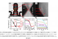
Research on vertical nanometer gate-all-around devices at the Institute of Microelectronics has achieved another breakthrough​


In advanced integrated circuit manufacturing processes , nanogate-all-around devices ( GAA ) are replacing FinFETs as the core devices in integrated circuits. Vertical nanometer gate-all-around devices have become an important research direction in advanced logic and DRAM technology due to their unique advantages in reducing standard cell area, easing gate length restrictions, increasing integration density , and improving parasitic capacitance / resistance.

  Zhu Huilong’s research team at the Institute of Microelectronics’ Integrated Circuit Leading Process R&D Center first proposed a self-aligned metal gate vertical gate-all-around nanotransistor in 2016 and conducted a systematic study on it. It has achieved great results in terms of device structure, process, integration technology and application. Through a series of progress and breakthroughs, the research and development results such as VSAFET , VCNFET , Fe-VSAFET , and 3D NOR have been published in top international journals in the field of microelectronic devices, and have been featured as covers or "Editor's Choice" articles many times.

  Recently, the team used a self-developed self-limiting ALE ( atomic layer etching ) process to achieve dual selective and precise etching of germanium-silicon materials and crystal planes by germanium , and prepared a silicon wafer composed of (111) crystal planes. Hourglass-shaped single crystal Ge channel self-aligned vertical nanometer gate-all-around device. The narrowest point of this hourglass-shaped Ge channel device is 5-20nm, showing excellent immunity to short channel effects and other excellent properties . The on-state current (I on ) of the nanowire device reaches 291μA/μm , which is the largest among similar devices. The device also has a high current switching ratio (I on /I off = 3.1×10 6 ) , good sub-threshold swing (SS = 91 mV/dec ) and drain-induced barrier reduction (DIBL = 55mV/V ) . Relevant research results were published in ACS NANO , a top journal in engineering technology ( 2023 Impact Factor /JCR Division: 17.1/Q1 ) (DOI: 10.1021/acsnano.3c02518). Xie Lu, a doctoral student at the Pioneer Center, is the first author of the article , and Researcher Zhu Huilong He and Senior Engineer Zhang Yongkui are the co-corresponding authors.

  The research was funded by the Strategic Priority Project of the Chinese Academy of Sciences, the Youth Innovation Promotion Association of the Chinese Academy of Sciences, the Beijing Superstring Memory Institute, and the National Natural Science Foundation of China.

1699974110791.png

Please, Log in or Register to view URLs content!
 

tokenanalyst

Brigadier
Registered Member

China Electronics Technology Nanjing Epitaxial Materials Industrial Base announced that it was officially put into operation​

Recently, a major science and technology industry project was officially put into operation in Nanjing. China Electronics Semiconductor Materials Co., Ltd. Nanjing Epitaxial Materials Industrial Base, a project located in Nanjing Jiangning Development Zone, has now been successfully put into production after a construction period of less than two years.

The project was signed and settled on September 27, 2021. It is located in the Comprehensive Bonded Zone of Jiangning Development Zone and covers an area of approximately 100,000 square meters. The establishment of this industrial base will not only effectively promote the development of my country's semiconductor industry, but also inject new vitality into the development of the technology industry in Nanjing and surrounding areas.

According to information from Zijinshan Observation, the investment in the first phase of the project is as high as 1.93 billion yuan. After the project reaches production, it is estimated that the new annual revenue will reach 2.5 billion yuan. This will create a production capacity of 4.56 million 8-12-inch silicon epitaxial wafers/year and 126,000 6-8-inch compound epitaxial wafers/year.

Please, Log in or Register to view URLs content!
 

tokenanalyst

Brigadier
Registered Member

Silxin releases self-developed digital circuit debugging software "Xin Shen Jue"​


On November 10, 2023, at ICCAD 2023, for thousands of upstream and downstream companies and people in the EDA industry present, Sierxin, a well-known digital EDA supplier in the industry, officially released a self-developed digital circuit debugging software- " "Core Spiritual Awareness"

This new tool integrates core functions such as source code tracking, waveform debugging, schematic extraction and coverage analysis , aiming to provide engineers with a comprehensive and efficient analysis and debugging platform. Use advanced debugging technology to help developers simplify the entire debugging process and accelerate chip development.

In the field of digital circuit design and verification, visual debugging tools are a powerful tool for engineers to locate code problems, and are now the mainstream debugging tools for verification engineers. With the rapid advancement of integrated circuit technology, the size and complexity of designs continue to increase, which brings new challenges to debugging work. Modern electronic design often requires multi-level verification, from RTL design to gate level to transmission level, and diverse design environments increase the complexity of debugging. Engineers need to switch between different environments to ensure accurate transmission of data and status. In order to meet this challenge, debugging tools need to be able to span different design environments and provide a unified debugging interface to reduce the time engineers spend switching between different environments, simplify the debugging process, and improve debugging efficiency.

It is against this background that Xinshenjue came into being. It not only provides engineers with a comprehensive and efficient analysis and debugging platform, but also meets the needs of mainstream verification and debugging scenarios through efficient source code tracking and key debugging functions. . Its interface design is simple and intuitive, with fast response speed and stable operation, providing engineers with an extremely convenient user experience and powerful debugging support.

1699976993622.png

Please, Log in or Register to view URLs content!
 
Status
Not open for further replies.
Top