You are using an out of date browser. It may not display this or other websites correctly.
You should upgrade or use an alternative browser.
You should upgrade or use an alternative browser.
Chinese semiconductor industry
- Thread starter Hendrik_2000
- Start date
- Status
- Not open for further replies.
They could integrate from domestic suppliers Like U-Precision, CNEPO, Cheertech, RSLaser and others. Also suppliers like Karl Zeiss could also expand their production inside China.ASML is just an integrator. There would be little advantage in them having a factory in China if the major components like the optics and light source are still imported.
i have seen zero indication that they ever intend to do soThey could integrate from domestic suppliers Like U-Precision, CNEPO, Cheertech, RSLaser and others. Also suppliers like Karl Zeiss could also expand their production inside China.
The problem with SMEE is not the components but the integration itself, is WAY more complex than putting things together, for example ASML overlay system, the thing that allows fabs to make multipattern is brutal, that development of that system falls into ASML hands and probably from all I have been seeing has been one of the biggest headache and delays that SMEE has faced.If the Chinese component suppliers could handle the job, then the SMEE litho machine would be in service right now.
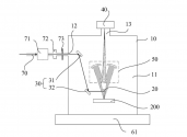
Is that the right caption for the patent image? The patent describes a mask defect detection device, so it’s more like an inspection tool…FEL-SSMB EUV litho machine
Is that the right caption for the patent image? The patent describes a mask defect detection device, so it’s more like an inspection tool…
-in a first aspect of the present invention, a mask defect inspection apparatus is provided, including: the mask to be detected is arranged in the vacuum cavity, and an injection port and an ejection port through which an extreme ultraviolet light beam passes are arranged on the shell
-In a second aspect of the present invention, a mask defect inspection system is provided, where the mask defect inspection system includes: a plurality of mask defect inspection devices according to the first aspect;
- In a third aspect of the present invention, a lithography system is provided, including: the mask defect detecting system in the second aspect solution; and each photoetching machine is communicated with one sub-beam output pipeline in the mask defect detection system, and an extreme ultraviolet light emitting device in the mask defect detection system supplies an extreme ultraviolet beam to the photoetching machine through a light splitting device.
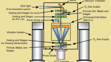
Also the picture of the patent is oddly similar to this:

A EUV projection objective, which its main function is to project the reduced image of the EUV mask into the coated wafer.
The emphasis on mask inspection is probably more due the lack of euv pellicles.
It looks like they are using this device as an EUV patterning device and EUV metrology tool, makes logic, SSMB and FELs are so powerful that could probably power multiple of these devices in a row, for both metrology and patterning.
- Status
- Not open for further replies.


