Chinese semiconductor industry

Status
Not open for further replies.

tokenanalyst

Brigadier
Registered Member

Based on diamond semiconductor materials, Pingmei Shenma started a new 400 million yuan project​

on October 31, the groundbreaking ceremony of Pingmei Shenma's 1 million carat annual CVD diamond functional material project was held in the Advanced Manufacturing Development Zone of Guangshan County, Xinyang City, Henan Province.
News from China Pingmei Shenma Group shows that the total investment in the project is about 400 million yuan. Based on the development status of the diamond semiconductor material industry and the needs of various industries, it will vigorously develop diamond-based silicon wafer materials and CVD diamond film technology and diamond ultra-wide band gap semiconductor functional materials, etc., realize the upgrading of production technology.
The deputy general manager of China Pingmei Shenma Group said that the construction of the project is in line with China Pingmei Shenma Group’s planning goals of becoming bigger, stronger and developing a complete diamond industry chain. After the project is completed , it will increase the market share of carbon-based substrates for high-end wafer-level power devices in China

Please, Log in or Register to view URLs content!
 

tokenanalyst

Brigadier
Registered Member

AMEC demonstrates MOCVD technology to achieve high crystal quality GaN thin film epitaxy​


Recently, AMEC demonstrated its advanced MOCVD (Metal Organic Chemical Vapor Deposition) technology at the 5th National Wide Bandgap Semiconductor Academic Conference, successfully achieving high crystal quality GaN (gallium nitride) thin film epitaxy.

The MOCVD equipment Prismo UniMax developed by China Microelectronics Corporation uses PVD AlN (aluminum nitride) and low-temperature gallium nitride composite buffer layer technology to successfully achieve high crystal quality GaN thin film epitaxy. In addition, AMEC also used 8'' silicon substrates for LED growth on stand-alone chip MOCVD equipment. By introducing an AlN/AlGaN buffer layer and using a real-time in-situ warpage monitoring system, the wafer stress was accurately controlled and successfully achieved 8'' silicon-based blue LED that achieves high wavelength uniformity.

These achievements demonstrate AMEC's leading position in MOCVD technology and GaN thin film epitaxy, and provide strong support for the development of high-end display applications such as Mini/Micro-LED. AMEC's technological innovation and large-size epitaxial growth technology are expected to further promote the development of the wide-bandgap semiconductor industry.

AMEC has always been committed to promoting technological innovation, working closely with upstream and downstream enterprises in the industry chain to accelerate technological innovation and jointly promote the vigorous development of the third-generation semiconductor industry. In the future, China Microelectronics will continue to aim at the world's technological frontier, keep up with industry development trends, adhere to the "Four Ten" corporate culture, and continue to promote the three-dimensional development strategy.

Please, Log in or Register to view URLs content!
 

tokenanalyst

Brigadier
Registered Member

Northern Huachuang's net profit surged 71.06% in the first three quarters, reaching 2.884 billion yuan​

Northern Huachuang recently announced its performance report for the first three quarters of 2023. The report shows that the company's operating income during this reporting period reached 14.588 billion yuan, a year-on-year increase of 45.70%; the net profit attributable to the parent company was as high as 2.884 billion yuan, a year-on-year increase of 71.06%.

In the third quarter, Northern Huachuang achieved operating income of 6.161 billion yuan, a year-on-year increase of 34.88%; net profit attributable to the parent company was 1.085 billion yuan, a year-on-year increase of 16.48%.

Northern Huachuang said that in the first three quarters of 2023, the company's market share of semiconductor equipment business has steadily increased, and operating efficiency has continued to improve. This enabled the company's total operating income and net profit attributable to shareholders of listed companies to continue to grow compared with the same period last year.

As a leading domestic supplier of semiconductor equipment and electronic components, North Huazhuang has been committed to product research and development, production, sales and technical services. Its semiconductor equipment business covers core process equipment such as etching, thin film, cleaning, heat treatment, and crystal growth, which are widely used in various semiconductor manufacturing processes.

In addition, Northern Huachuang also has profound technological accumulation in the fields of vacuum and lithium battery equipment. The products it develops include crystal growth equipment, vacuum heat treatment equipment, atmosphere protection heat treatment equipment, etc., which are widely used in material heat treatment, vacuum electronics, new energy photovoltaics, semiconductor materials, magnetic materials, new energy vehicles and other fields.

Northern Huachuang also has outstanding performance in the field of precision electronic components. The products it develops include quartz crystal devices, quartz microelectromechanical sensors, high-precision resistors, etc., which are widely used in high-speed rail, smart grids, communications, medical electronics, precision instruments, automatic control and other fields.

With the continuous development of technology, the demand for semiconductor equipment and electronic components will continue to grow. As an industry leader, Northern China is expected to continue to maintain strong growth momentum in the coming years.

Please, Log in or Register to view URLs content!
 

tphuang

Lieutenant General
Staff member
Super Moderator
VIP Professional
Registered Member

AMEC demonstrates MOCVD technology to achieve high crystal quality GaN thin film epitaxy​


Recently, AMEC demonstrated its advanced MOCVD (Metal Organic Chemical Vapor Deposition) technology at the 5th National Wide Bandgap Semiconductor Academic Conference, successfully achieving high crystal quality GaN (gallium nitride) thin film epitaxy.

The MOCVD equipment Prismo UniMax developed by China Microelectronics Corporation uses PVD AlN (aluminum nitride) and low-temperature gallium nitride composite buffer layer technology to successfully achieve high crystal quality GaN thin film epitaxy. In addition, AMEC also used 8'' silicon substrates for LED growth on stand-alone chip MOCVD equipment. By introducing an AlN/AlGaN buffer layer and using a real-time in-situ warpage monitoring system, the wafer stress was accurately controlled and successfully achieved 8'' silicon-based blue LED that achieves high wavelength uniformity.

These achievements demonstrate AMEC's leading position in MOCVD technology and GaN thin film epitaxy, and provide strong support for the development of high-end display applications such as Mini/Micro-LED. AMEC's technological innovation and large-size epitaxial growth technology are expected to further promote the development of the wide-bandgap semiconductor industry.

AMEC has always been committed to promoting technological innovation, working closely with upstream and downstream enterprises in the industry chain to accelerate technological innovation and jointly promote the vigorous development of the third-generation semiconductor industry. In the future, China Microelectronics will continue to aim at the world's technological frontier, keep up with industry development trends, adhere to the "Four Ten" corporate culture, and continue to promote the three-dimensional development strategy.

Please, Log in or Register to view URLs content!
I don't know if anyone else dometically has been able to do so, but having the domestic tools to be able to grow 8-inch GaN-on-Si wafers is pretty big deal

Not sure where they are on GaN-on-Sic
 

tphuang

Lieutenant General
Staff member
Super Moderator
VIP Professional
Registered Member

Based on diamond semiconductor materials, Pingmei Shenma started a new 400 million yuan project​

on October 31, the groundbreaking ceremony of Pingmei Shenma's 1 million carat annual CVD diamond functional material project was held in the Advanced Manufacturing Development Zone of Guangshan County, Xinyang City, Henan Province.
News from China Pingmei Shenma Group shows that the total investment in the project is about 400 million yuan. Based on the development status of the diamond semiconductor material industry and the needs of various industries, it will vigorously develop diamond-based silicon wafer materials and CVD diamond film technology and diamond ultra-wide band gap semiconductor functional materials, etc., realize the upgrading of production technology.
The deputy general manager of China Pingmei Shenma Group said that the construction of the project is in line with China Pingmei Shenma Group’s planning goals of becoming bigger, stronger and developing a complete diamond industry chain. After the project is completed , it will increase the market share of carbon-based substrates for high-end wafer-level power devices in China

Please, Log in or Register to view URLs content!
keep your eyes on this, huge national security implications.

if you can get diamond power semiconductor cost down, then you can just skip the Gallium oxide AESA radar and go straight to diamond ones, lol

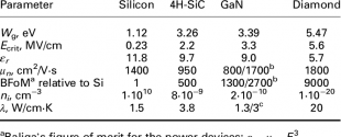
Please, Log in or Register to view URLs content!

DiamondVsGaNVsSic.png
Look at the bandgap value there 5.47, even higher than gallium oxide (4.8 I think)
 

mst

Junior Member
Registered Member

Chinese scientists create chip than can perform AI task 3,000 times faster than Nvidia’s A100: study.​

Although the new chip cannot immediately replace those used in devices such as computers or smartphones, it may soon be used in wearable devices, electric cars or smart factories and help boost China’s competitiveness in the mass application of
Please, Log in or Register to view URLs content!
, researchers wrote in a paper published in the journal Nature.
Please, Log in or Register to view URLs content!
 

99PLAAFBalloons

New Member
Registered Member

Chinese scientists create chip than can perform AI task 3,000 times faster than Nvidia’s A100: study.​

Already posted by @tokenanalyst , see:

The Department of Automation and the Department of Electronics collaborate to develop ultra-high-speed optoelectronic computing chips​

Tsinghua News Network, October 30. In 1965, Gordon Moore, one of the founders of Intel, proposed "Moore's Law" that has influenced the chip industry for more than half a century: it predicts that the number of transistors that an integrated circuit can accommodate will increase every two years or so. Double. The field of semiconductors has prospered and developed under Moore's Law for decades, and "chips" have become an important engine for mankind to enter the intelligent era. However, as transistor size approaches physical limits, Moore's Law has slowed down or even faced failure in the past decade. How to build a new generation of computing architecture and establish a "new" order for chips in the artificial intelligence era has become a frontier hot topic of great concern to the international community.

In response to this problem, Academician Dai Qionghai and Assistant Professor Wu Jiamin of the Department of Automation of Tsinghua University, and Associate Professor Fang Lu and Associate Researcher Qiao Fei of the Department of Electronic Engineering jointly tackled the problem and proposed a new computing architecture that "breaks away" from Moore's Law: optoelectronic simulation chips, computing power Reaching more than 3,000 times that of current high-performance commercial chips. The relevant results are titled "All-analog photo-electronic chip for high-speed vision tasks " and were published in the journal Nature in the form of a long article . If the running time of a vehicle is used to compare the information flow calculation time in a chip, then the emergence of this chip is equivalent to shortening the 8-hour running time of the Beijing-Guangzhou High-speed Railway to 8 seconds.

In this small chip, the Tsinghua University research team creatively proposed a computing framework for deep integration of optoelectronics. Starting from the most essential physical principles, it combines optical computing based on electromagnetic wave space propagation and pure analog electronic computing based on Kirchhoff's laws, "breaking away" from the physics that restricts data conversion speed, accuracy and power consumption in traditional chip architectures. The bottleneck is to break through three international problems of large-scale computing unit integration, high-efficiency nonlinearity, and high-speed optical and electrical interfaces on one chip.
View attachment 120800
Optoelectronic chip
According to actual measurement performance, the system-level computing power of the optoelectronic fusion chip is thousands of times higher than that of the existing high-performance chip architecture. However, such amazing computing power is only one of the many advantages of this chip.

In the intelligent vision tasks and traffic scene calculations demonstrated by the R&D team, the system-level energy efficiency (number of operations that can be performed per unit energy) of the optoelectronic fusion chip was measured to reach 74.8 Peta-OPS/W, which is more than 4 million peta-OPS/W of existing high-performance chips. times. To put it figuratively, the amount of electricity that originally powered an existing chip to work for one hour can last it more than 500 years.

A key factor currently limiting the limits of chip integration is the heat dissipation problem caused by excessive density. Optoelectronic fusion chips operating at ultra-low power consumption will help greatly improve chip heating problems and bring all-round breakthroughs to future chip designs.

Furthermore, the minimum processing line width of the optical part of the chip is only one hundred nanometers, while the circuit part only uses 180nm CMOS process, which has achieved performance improvements of several orders of magnitude compared to high-performance chips made using the 7nm process. At the same time, the materials used are simple and easy to obtain, and the cost is only a few tenths of the latter.

Please, Log in or Register to view URLs content!
Direct paper link:
Please, Log in or Register to view URLs content!
(non-paywalled)
 
Status
Not open for further replies.
Top