Chinese semiconductor industry

Status
Not open for further replies.

KYli

Brigadier
They still think they could stop China from expanding its capacity for legacy chips.
Please, Log in or Register to view URLs content!
Some Chinese foundational chips are already priced 20% to 30% cheaper than offerings from foreign rivals, according to Silverado’s report. At one point in 2022, Chinese chipmaker GigaDevice Semiconductor Inc. was charging only about one-fourth of what STMicroelectronics NV was asking for comparable products in China, according to a chart in the report attributed to Minsheng Securities.

The US and its European allies are worried that China could eventually dump those cheaper chips on the global market or use them as political leverage. But so far, the Biden administration has focused its policy efforts on just the most advanced chips and equipment — technology it fears will give China a military edge.


To counter undercutting before it’s too late, Silverado said, the US should use investment review and trade investigation tools — as well as gather better pricing and product data — to defend chipmakers in America and allied nations. The report also suggested that the US use export controls to limit shipments of chipmaking technology, not just for advanced chips but for older varieties as well.
 

tokenanalyst

Brigadier
Registered Member
They still think they could stop China from expanding its capacity for legacy chips.
Please, Log in or Register to view URLs content!
Some Chinese foundational chips are already priced 20% to 30% cheaper than offerings from foreign rivals, according to Silverado’s report. At one point in 2022, Chinese chipmaker GigaDevice Semiconductor Inc. was charging only about one-fourth of what STMicroelectronics NV was asking for comparable products in China, according to a chart in the report attributed to Minsheng Securities.

The US and its European allies are worried that China could eventually dump those cheaper chips on the global market or use them as political leverage. But so far, the Biden administration has focused its policy efforts on just the most advanced chips and equipment — technology it fears will give China a military edge.


To counter undercutting before it’s too late, Silverado said, the US should use investment review and trade investigation tools — as well as gather better pricing and product data — to defend chipmakers in America and allied nations. The report also suggested that the US use export controls to limit shipments of chipmaking technology, not just for advanced chips but for older varieties as well.
Yeah the clock has been set, it's doesn't matter what Gina said, is only a matter of time until marco rubio and the other stooges start screeching loud enough to start export controlling "mature equipment" too, if not in this administration, the next one.

So now is up to China industrialists to decide if they want to wait until the last hour until everything is banned to start procuring and collaborating with domestic suppliers.


tphuang

Lieutenant General
Staff member
Super Moderator
VIP Professional
Registered Member
Screen Shot 2023-10-26 at 2.57.23 PM.png
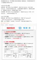
well, depending on how much you believe this stuff, but this is Huawei Ascend-910B apparently being used to train Zhipu AI in comparison with A100.

In both cases, I'm assuming 8 card and using PyTorch. This seems to match what Huawei itself claimed before. i think MindSpore + Ascend-910 would yield better numbers.

Basically, it looks like they are about the same for ChatGLM-6B and 910B was a little worse for GLM-130B
 

tphuang

Lieutenant General
Staff member
Super Moderator
VIP Professional
Registered Member
I have no doubt at this point the fabs themselves are juggling a medium between de-risking vs trying to maintain their operations. After all, there is still the need to supply the local market.

So unless people here have evidence that they are not de-risking, I'm not sure what the point of keep speculating on whether or not they are using domestic machines.

More importantly, Domestic SMEs don't have the capacity to supply all the fabs. They are ramping up production, but it takes time. It takes time to hire and train people
 

tokenanalyst

Brigadier
Registered Member

Chongqing sets up a 30 billion yuan industrial development fund to focus on intelligent connected new energy vehicles, integrated circuits, etc.​


On October 26, the 2023 Chongqing Venture Capital Conference "Financial Empowerment Industry·Technology-led Development" officially opened. The conference was co-sponsored by Chongqing Financial Supervision Bureau, Chongqing Science and Technology Bureau, Western Science City Chongqing High-tech Zone, and Zero2IPO Entrepreneurship.

At the meeting, the Western (Chongqing) Science City Industrial Development Fund (hereinafter referred to as the Fund) was officially launched. The total scale of the fund is 30 billion yuan, which aims to leverage social capital, increase investment of "real money", and attract and gather innovative companies. investment institutions, accelerate the formation of an overall, multi-level, high-quality industrial layout, and inject new impetus into the innovation-driven development of the Science City.

It is reported that the fund established this time is established by Chongqing High-tech Development Group and Xiyong Microelectronics Park Company as investors, and Gaorui Fund Management Company, a subsidiary of High-tech Development Group, is the manager. The first phase of the fund has a scale of 10 billion yuan. It will be operated in a market-oriented manner under the model of "parent fund + sub-fund + direct investment", and the scale will be enlarged twice through the parent fund and sub-fund. In terms of investment areas, it closely follows the "3238" modern manufacturing cluster system of Chongqing High-tech Zone, focusing on intelligent networked new energy vehicles and core devices, integrated circuits, biomedicine, new energy storage, aerospace information and other tracks. "Investment leads the way" and "investment promotes innovation" to promote the effective connection and two-way empowerment of industry and capital.

Please, Log in or Register to view URLs content!
 

interestedseal

Junior Member
Registered Member
@tphuag, With all due respect, I still think it's important I comment on @Weaasel's question. If you still think this is not good for this thread, feel free to remove this post.

I think everybody paid too much attention to litho tool as the bottleneck, and recently are giving lots of attention to the progress domestic WFE suppliers are making on etcher, deposition, wet process equipment, resists, and even EUV light source. I don't think people realize there are still many big gaps to fill in order to break the US restriction on advanced logic/DRAM/3D-NAND IC fabrication. Don't take my word at face value, I encourage you to investigate the list below to validate my concerns.

Potential bottleneck to reach self-sufficiency for Advanced Technology Nodes
Wafer:

Bright field wafer inspection
Dark field wafer inspection
ebeam inspection
diffraction based ADI Overlay metrology
AEI overlay metrology
CD SEM

Reticle:
advanced domestic merchant maskshops
reticle blanks
ebeam reticle writer
reticle etcher (Chrome & MoSi)
reticle blank inspection (should be relatively easy to overcome)
reticle inspection
reticle CD SEM
reticle registration metrology
reticle repair tool
AIMS
pellicles
curvilinear OPC for EUV reticles
multibeam reticle writer for EUV
EUV reticle blanks
EUV pellicle

Maybe it's just me, but I couldn't find much information on domestic WFE working on the above toolsets for <=16nm logic / <=18nm hp DRAM / >=128L 3D-NAND. Now that I've brought this to everyone' attention, perhaps you all could keep an eye out for relevant news or info. With more people looking it may be faster for us to verify where we sit relative to advanced node needs. Note, we still have access to advanced reticles from the Japanese maskshops, the reticle fabrication equipment I outlined would only come into play as bottleneck if the U.S. blocks sale of advanced reticles to China.
At least three companies have unveiled overlay metrology tools. Yuwei’s Houyi series might be image-based, but Angstrom’s tool has been confirmed to be diffraction based.
Please, Log in or Register to view URLs content!
 

tokenanalyst

Brigadier
Registered Member
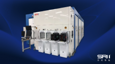
The only tool that people often say is as complex as a immersion lithography machines is an Ion Implantation tool and China already has three of those companies already CTEC(Semicores), Wanye(Kingstone) and SRI-I

1698363550402.png

In theory if SMEE undisclosed immersion scanners can give a least some decent throughput and a decent overlay, I could say that you could built a 28nm fab all domestic, of course we are not talking something even close to TSMC gigafabs.
And I could believe that they already doing that to test and solved problems in the domestic supply chain. Simply makes sense.
 

tokenanalyst

Brigadier
Registered Member

The important progress made by Professor Chen Rong's team in selective atomic layer deposition has facilitated the high-precision self-aligned manufacturing process of advanced integrated circuit processes.​


On July 26, Professor Chen Rong’s team in our laboratory published a paper in Nature Communications entitled "Self-aligned patterning of tantalum oxide thin films on Cu/SiO2 surface through redox-coupled intrinsically selective atomic layer deposition method. " (Self-Aligned Patterning of Tantalum Oxide on Cu/SiO2through Redox-coupled Inherently Selective Atomic Layer Deposition) important research progress. Dr. Li Yicheng and doctoral student Qi Zilian of Huazhong University of Science and Technology are the co-first authors of the paper. Professor Chen Rong and Associate Professor Cao Kun of our laboratory are the co-corresponding authors of the paper. Huazhong University of Science and Technology is the first unit to complete the thesis, and Hubei Jiangcheng Laboratory is the cooperative unit.
408E47EBB8095DC22C83F67EE6A_6342C009_1697F.png

With the development of integrated circuit manufacturing technology and market demand, the feature size of chips has shrunk and the interconnection density has further increased. The self-aligned manufacturing of chips requires a complex process of multiple depositions, photolithography, and etching. The steps are many and the cost is high. Leakage and short circuit of adjacent metal wires caused by overlay errors is a technical problem in advanced manufacturing processes. The research team developed a solution for self-aligned deposition of high-precision thin films. They used selective atomic layer deposition technology to achieve self-aligned growth of the target dielectric layer on the bottom dielectric layer, without growing on the metallic copper surface in the non-growth area. This process reaches a thickness of 5 nanometers in the growth area, no growth in the non-growth area, and the selectivity reaches 100%, achieving self-aligned deposition. The importance of this technology to the field is reflected in the fact that for advanced chip manufacturing processes, it can improve alignment accuracy, reduce photolithography and etching steps, and improve chip process yields.
2FA31A83CD68707AFEAF4A4D639_C1AAC195_E8EC.png

Self-aligned deposition patterned thin film technology route, selective deposition effectively reduces the complex steps of multiple photolithography and etching, and improves self-alignment accuracy

This work found that different oxidation states of the copper surface will cause the formation of defect sites on the surface of the non-growth area, and these nucleation defects lead to the loss of selectivity. The research team broke through the conventional ALD two-step cycle alternating growth, added an in-situ reduction and correction step, and proposed a "cycle coupling" process that transformed the traditional AB double cycle into an ABC multi-cycle coupling, thereby enabling in-situ surface reduction-growth- The defect removal step effectively suppresses the nucleation of defects on the copper surface and ultimately achieves high-precision self-alignment.
 
Status
Not open for further replies.
Top