Chinese semiconductor industry

Status
Not open for further replies.

tokenanalyst

Brigadier
Registered Member

Lucent Wafer Manufacturing Virtual Simulation Training System​

Hangzhou Luxun Technology Co., Ltd. officially released a wafer manufacturing virtual simulation training system. The system uses virtual simulation and virtual reality technology to conduct high-level simulations of the workshop environment, real equipment, process flow, etc. according to the requirements of the real FAB line environment for 8-inch wafers, mainly including single crystal silicon growth, silicon substrate preparation, oxidation, There are 9 major processes including photolithography, etching, ion implantation, chemical vapor deposition (CVD), physical vapor deposition (PVD), and chemical mechanical polishing (CMP). The system uses a 3D immersive interactive method to allow students to experience and participate in the overall process, parameter setting and other technical processes, and then master the basic principles of the integrated circuit manufacturing process, equipment understanding, process training and parameter setting and other technical skills.
As a well-known domestic integrated circuit testing professional service company and a typical integrated circuit industry-education integrated enterprise, Lanxun Technology adheres to the vision of building a world-class integrated circuit testing base and continuing to empower "China Chip" with advanced technology and innovative models. , focusing on the ecological construction and services of the integrated circuit industry, the integration of industry and education, and talent training, to help the national integrated circuit industry achieve high-level technological self-reliance and self-reliance.
In March this year, Luxun Technology's virtual simulation R&D team conducted a month-long in-depth survey and interviews on the offering status and teaching models of integrated circuit-related professional courses in nearly 100 domestic colleges and universities. In early April, our company officially launched the development of a wafer manufacturing virtual simulation training system to specifically solve the pain points of "high investment, high difficulty, high risk, difficulty in implementation, difficulty in observation, and difficulty in reproduction" in the practical training and teaching process. and difficult problems to effectively realize the informatization, intelligence and modernization of talent training.
The wafer manufacturing virtual simulation training system is a further improvement of the full-link virtual simulation training system. It can effectively link the packaging training system and the testing training system, and ultimately realize a complete closed-loop integrated circuit training operation. At the same time, interested schools can contact our company for product experience and trial!

Please, Log in or Register to view URLs content!
 

hvpc

Junior Member
Registered Member
For projection steppers I think they use the same mercury vapor lamps but frontend I-line scanners their field I think is too small for packaging and also is too expensive for packaging because these scanners use pretty sophisticated systems to archive high accuracy, In the case of ASML is less than 20nm.

For packaging the overlay accuracy is lower, about 50-100nm and also the NA of the optics is lower because a wider image is more important in packaging than a very high resolution. The recently launched SSB520 packaging lithography stepper has a resolution of less than 600nm and accuracy of 100nm but the field is like 4 times the standard IC size. Canon Packaging Steppers are pretty similar.
The industry look at frontend (FE) and backend (BE) litho as distinct products.

Backend steppers could be i/g/h line, with magnification of 1X or 2X, and like you mentioned, larger field size.

FE are typically 4X magnification scanners; BE are typically i/g/h-line steppers with 1X or 2X magnification

FE litho focus is on resolution so targets larger NA projectio lens; BE needs larger Depth of Focus (DoF) so needs larger NA. BE litho supports thicker substrates up to 2mm.

0.35um technology node FE appliction uses FE iline steppers with 5X magnification. Backend iLine stepper is not capable of supporting any FE litho needs.

SMEE SSB500/40 & SSB500/50, their primary backend litho tools are 1X i/g/h-line stepper with resolution limit of 2um & 1um; Single Machine Overlay (SMO) of 0.3um & MMO of 0.6um. DoF spec is 8um for 1um feature size & 30um for 3um features. and have very slow throughput <100 wafers-per-hour.

BE steppers are not the same and not in the same class as a high-precision, highly efficient FE scanners, and this shows in the unit price of these machines. So no matter you arguing the technical merit that both are litho tools, they are not the same and viewed as seperate and distinct types of machines.
 

tokenanalyst

Brigadier
Registered Member
The industry look at frontend (FE) and backend (BE) litho as distinct products.

Backend steppers could be i/g/h line, with magnification of 1X or 2X, and like you mentioned, larger field size.

FE are typically 4X magnification scanners; BE are typically i/g/h-line steppers with 1X or 2X magnification

FE litho focus is on resolution so targets larger NA projectio lens; BE needs larger Depth of Focus (DoF) so needs larger NA. BE litho supports thicker substrates up to 2mm.

0.35um technology node FE appliction uses FE iline steppers with 5X magnification. Backend iLine stepper is not capable of supporting any FE litho needs.

SMEE SSB500/40 & SSB500/50, their primary backend litho tools are 1X i/g/h-line stepper with resolution limit of 2um & 1um; Single Machine Overlay (SMO) of 0.3um & MMO of 0.6um. DoF spec is 8um for 1um feature size & 30um for 3um features. and have very slow throughput <100 wafers-per-hour.

BE steppers are not the same and not in the same class as a high-precision, highly efficient FE scanners, and this shows in the unit price of these machines. So no matter you arguing the technical merit that both are litho tools, they are not the same and viewed as seperate and distinct types of machines.
Still optical projection lithography.
 

BoraTas

Captain
Registered Member
The industry look at frontend (FE) and backend (BE) litho as distinct products.

Backend steppers could be i/g/h line, with magnification of 1X or 2X, and like you mentioned, larger field size.

FE are typically 4X magnification scanners; BE are typically i/g/h-line steppers with 1X or 2X magnification

FE litho focus is on resolution so targets larger NA projectio lens; BE needs larger Depth of Focus (DoF) so needs larger NA. BE litho supports thicker substrates up to 2mm.

0.35um technology node FE appliction uses FE iline steppers with 5X magnification. Backend iLine stepper is not capable of supporting any FE litho needs.

SMEE SSB500/40 & SSB500/50, their primary backend litho tools are 1X i/g/h-line stepper with resolution limit of 2um & 1um; Single Machine Overlay (SMO) of 0.3um & MMO of 0.6um. DoF spec is 8um for 1um feature size & 30um for 3um features. and have very slow throughput <100 wafers-per-hour.

BE steppers are not the same and not in the same class as a high-precision, highly efficient FE scanners, and this shows in the unit price of these machines. So no matter you arguing the technical merit that both are litho tools, they are not the same and viewed as seperate and distinct types of machines.
I never heard of BE litho getting used for FE either.

Still optical projection lithography.
An engineer or a corporation would gain useful knowledge from developing a BE litho which would probably be useful in developing a FE litho later. Yet this doesn't mean these technologies are the same or success in BE lithos would mean success in FE lithos.
 

tokenanalyst

Brigadier
Registered Member
I never heard of BE litho getting used for FE either.
I never say it does, I was responding to Tin Roberts saying that SMEE is not a lithography company, it may not be the frontend lithography company that we all want to SMEE to be, which is a disappointment, but is a lithography company. Backend projection lithography is still projection lithography and FPD projection lithography is still projection lithography, projection lithography for MEMS devices is still projection lithography.

An engineer or a corporation would gain useful knowledge from developing a BE litho which would probably be useful in developing a FE litho later. Yet this doesn't mean these technologies are the same or success in BE lithos would mean success in FE lithos.

I think as advanced packaging evolve and the features on IC packages substrates becomes denser and denser, packaging lithography machines in the near future could become very complex and costlier with more accurate overlays systems and algorithms, more accurate sensors, more complex optics and what i think will make things worse for these backend machines is that they are required to maintain a wide field for bigger package sizes while needing to increase the resolution. I think we should expect more overlapping between both types of machines in term of shared technologies.

In theory with the SSB520, that latest SMEE packaging lithography machine with a resolution of 0.6 microns and accuracy of 0.1 microns it could be possible build a 4004 processor or a MOS6052, considering that those processors were patterned using a microAlign projection lithography machine. In theory can also be done with Canon packaging machines.
 

BoraTas

Captain
Registered Member
very interesting
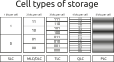
so QLC - quad layer cells
TLC - tri layer cells

So QLC - 4 bits per cell
TLC - 3 bits per cell

To me that would imply similar # of levels with QLC would have high bit density than TLC.

YMTC just seems so much more capable than CXMT

product info
Please, Log in or Register to view URLs content!
read 7000MB/s
write 6000MB/s

(does anyone know what these are?)
4k read 900KIOPS
4Kwrite 700KIOPS
You meant IOPS? Basically how many times a data of set size (4 kb is common) can be sent to/read from a device per second. A compound metric of access time of non-adjacent sections and bandwidth...

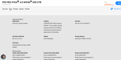
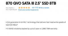
BTW QLC and TLC are not inherently superior to each other. Flash storages use floating-gate transistors whose working principle is based on a quantum effect. Very interesting stuff to read on if you are interested. QLC cells have 16 possible voltage levels which can be used to encode 4-bit data. TLC cells have 9 possible values. So non-binary computing has been here for a while for storage. Cells with less capacity are of longer lifespan and higher performance. For example the difference between Samsung PRO and, lower, QWO lines is Pro uses TLC instead of QLC.

1698192989669.pngPro TLC.png (ignore the Samsung guy)
Qwo GLC.png
 
Last edited:

hvpc

Junior Member
Registered Member
Still optical projection lithography.
: ). Haha. Ok.

By the way, I forgot to mention, when 0.35um was the leading edge node, I recall they were done on 5X iLine steppers. Using 1X stepper would put the strain on the mask makers as all the error on the mask no longer scale down 5X. This means mask guys would need to tighten all of their specifications by 5X.

Modern day FE steppers and scanners are so efficient with low cost/wafer that it wouldn’t make sense to use BE steppers as there’s no technical merit or cost savings from doing so.
 

Temstar

Brigadier
Registered Member
very interesting
so QLC - quad layer cells
TLC - tri layer cells

So QLC - 4 bits per cell
TLC - 3 bits per cell

To me that would imply similar # of levels with QLC would have high bit density than TLC.

YMTC just seems so much more capable than CXMT

product info
Please, Log in or Register to view URLs content!
read 7000MB/s
write 6000MB/s

(does anyone know what these are?)
4k read 900KIOPS
4Kwrite 700KIOPS
Cramming more bits into a cell is the primary way to increase NAND storage capacity. Both TLC and QLC are in vogue right now with penta level cells being developed and on the horizon, the controller for penta level cell NAND Is hella complicated though. There is a catch here - when writing new data into a cell you can't overwrite single bits at a time, the entire cell has to be overwritten. So the controller have to read out the whole cell, flip the bits it needs to change and then write the result back into that cell. This is why SSDs work faster when there's lot of free space remaining because the controller use the free space areas as a buffer to hold data to avoid having to juggle things around. Good controllers would even designate free area as "SLC (single level cell) mode" where only a single bit is written into cells that could hold 3 or 4 bit for use as a very fast cache area. "Overprovisioning" settings are same idea.

So with the above understanding we can say if your NAND is QLC it's easier to build a drive with greater storage capacity. With TLC its easier to build a drive with greater speed. Alternatively for a given capacity TLC drives are faster and more expensive as they have to have more cells than equivalent capacity QLC drives. Some current state of art drives for comparison:

Samsung 990 Pro - TLC, up to 7,450 / 6900 MB/s sequential read/write speed using NVMe PCIe 4.0 interface
Corsair MP600 CORE XT - QLC, up to 5,000 / 4,400MB/s sequential read/write speeds using NVMe PCIe 4.0 interface

This YMTC drive:
ZhiTai Ti600 - QLC, up to 7,000 / 6,000MB/s sequential read/write speeds using NVMe PCIe 4.0 interface

That's extremely fast for a QLC drive, approaching the speed of fastest TLC drive from Samsung.
 
Last edited:

tphuang

Lieutenant General
Staff member
Super Moderator
VIP Professional
Registered Member
You meant IOPS? Basically how many times a data of set size (4 kb is common) can be sent to/read from a device per second. A compound metric of access time of non-adjacent sections and bandwidth...

BTW QLC and TLC are not inherently superior to each other. Flash storages use floating-gate transistors whose working principle is based on a quantum effect. Very interesting stuff to read on if you are interested. QLC cells have 16 possible voltage levels which can be used to encode 4-bit data. TLC cells have 9 possible values. So non-binary computing has been here for a while for storage. Cells with less capacity are of longer lifespan and higher performance. For example the difference between Samsung PRO and, lower, QWO lines is Pro uses TLC instead of QLC.

View attachment 120549View attachment 120550 (ignore the Samsung guy)
View attachment 120551
yes 900k IOPS and 700k IOPS in that case.

I don't doubt that there are benefits with fewer bits per cell, but I would think that if they got I/O speed to such a competitive level, then QLCs advantage in bit per layer would translate to noticeable lower cost per GB of storage.

It might be a reason YMTC is able to price its SSDs cheaper than Samsung & SK.
 

hvpc

Junior Member
Registered Member
yes 900k IOPS and 700k IOPS in that case.

I don't doubt that there are benefits with fewer bits per cell, but I would think that if they got I/O speed to such a competitive level, then QLCs advantage in bit per layer would translate to noticeable lower cost per GB of storage.

It might be a reason YMTC is able to price its SSDs cheaper than Samsung & SK.
QLC wear out faster than TLC.

The recent cheaper SSD price at the moment is mostly due to macroeconomic. When the supply/demand dynamic regress to healthy level the cost-per-bit is expected to increase back to “normal”. In fact, Flash price has been ticking upwards the last few weeks.
 
Status
Not open for further replies.
Top