Shanghai Microsystems Institute achieves breakthrough in 300 mm SOI wafer manufacturing technology
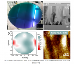
Recently, the team of researcher Wei Xing of Shanghai Institute of Microsystems has made breakthrough progress in 300 mm SOI wafer manufacturing technology and prepared the first 300 mm radio frequency ( RF ) SOI wafer in China. Based on the 300 mm SOI R&D platform of the National Key Laboratory of Integrated Circuit Materials, the team successively solved the preparation of low-oxygen high-resistance crystals, low-stress high-resistivity polysilicon film deposition, and non-contact planarization required for 300 mm RF-SOI wafers. Many core technical problems have achieved a major breakthrough in domestic 300mm SOI manufacturing technology from scratch.

At present, RF-SOI wafers have become the mainstream substrate material for radio frequency applications, accounting for more than 90% of the market share of radio frequency front-end chips such as switches, low-noise amplifiers and tuners . With the full rollout of 5G networks, the demand for RF modules in mobile terminals continues to increase. The RF front-end chip manufacturing process is transitioning from 200 mm to 300mm RF-SOI . Taking this opportunity, domestic mainstream integrated circuit manufacturing companies are also actively expanding into 300mm . RF-SOI process foundry capability. Therefore, the independent preparation of 300 mm RF-SOI wafers will effectively promote the coordinated and rapid development of the entire domestic RF-SOI chip design, foundry and packaging industry chain, and provide a solid guarantee for the supply security of domestic SOI wafers.
