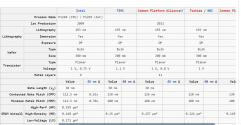
I have no idea where they are deriving the 28nm number from, does it mean that it can do 28nm wide features in a single exposure? Or does it mean that it can only reliably create features at 28nm and above?Why is it called 28nm? It's immersion, so it should be capable of 14nm and even 7nm nodes right?
You are using an out of date browser. It may not display this or other websites correctly.
You should upgrade or use an alternative browser.
You should upgrade or use an alternative browser.
Chinese semiconductor industry
- Thread starter Hendrik_2000
- Start date
- Status
- Not open for further replies.
I have no idea where they are deriving the 28nm number from, does it mean that it can do 28nm wide features in a single exposure? Or does it mean that it can only reliably create features at 28nm and above?
28nm denotes overlay accuracy,according to havok
on the SSA800 article, I think it's important if we can find the original Chinese source on this. Again, the word on the street is that the first delivery will be happening soon, but I always find it unlikely for them to make an official announcement of it. I will see if I can find that today
It means it can do 28nm in a single pass. With multi-patterning it should be capable of lower, all the way to 7nm they're saying.Why is it called 28nm? It's immersion, so it should be capable of 14nm and even 7nm nodes right?
To explain, but I am not being accurate here. If one pass can do 28nm, then 2 passes with masks could do 14nm and 4 passes could do 7nm. The problem is, but the more passes you do, the less accurate your going to be. This is the yield rate they keep talking about. More passes usually means less yield.
Note, this is true for EUV as well. The ASML EUV does 14nm per pass. They get to 3nm using multi-patterning. This is why Samsung's and TSMC's yield rate on 3nm is so horrible.
And if you really want your mind blown, the actual light SMEE's SA800 is actually 193nm.
broadsword
Brigadier
I think that you should have a posting that informs people of the basics of IC chip manufacturing starting from smelting of silicon ores such as silica, through ingot growing and unto the nitty gritty of the use of photomasks, different types of metrological instruments, and what the process of etching, ion implantation, vapour deposition, and photolithography are in a concise sequential manner. Also a succint explanation of SSMB and particle accelerators.
Manufacturing Process:
1)
2)
Originally posted by @latenlazy and another member whom I can't recall.
this weibo account can be on and off. Got kirin A2 right, but others not so much. Anyways, I think this post makes sense
so basically, expect Huawei to work on binary translation to migrate ecosystem from x86 to ARM, since it is preparing to be cutoff from Intel at some point手机有马良,PC有二进制翻译,目前就是把x86生态往ARM迁移,经过翻译后性能高度可用,到时候预计会配合HarmonyOS PC一起商用![[偷笑] [偷笑]](https://face.t.sinajs.cn/t4/appstyle/expression/ext/normal/71/2018new_touxiao_org.png)
I have no idea where they are deriving the 28nm number from, does it mean that it can do 28nm wide features in a single exposure? Or does it mean that it can only reliably create features at 28nm and above?
28nm is the process that the machine will by rated for, the physical resolution limit of immersion lithography is defined by 0.25 * 193nm / 1.35 NA = 35nm, in practice i think is closer to 45nm, so multi-patterning techniques like Double patterning and Quadruple patterning is required, that is basically controlled by the accuracy of the overlay technology, wafer metrology and computational lithography techniques.
28nm is the process that the machine will by rated for, the physical resolution limit of immersion lithography is defined by 0.25 * 193nm / 1.35 NA = 35nm, in practice i think is closer to 45nm, so multi-patterning techniques like Double patterning and Quadruple patterning is required, that is basically controlled by the accuracy of the overlay technology, wafer metrology and computational lithography techniques.
In this case, if physical resolution is closer to 40nm, then how are fabs able to do 28nm process with single exposure of Arfi scanner? At least that's what I've been led to believe with what we've discussed so far on this thread.
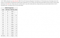
Well some parts of the process can be done using single patterning but overall multi-patterning has been the standard since the 32nm planar process, even with EUV, multi-patterning will be still a requirement because how the light behave.In this case, if physical resolution is closer to 40nm, then how are fabs able to do 28nm process with single exposure of Arfi scanner? At least that's what I've been led to believe with what we've discussed so far on this thread.

You can see in this table after 70nm+ TSMC use multi-patterning, my guess is that is easier to deal with overlay metrology issues than to deal light issues.

- Status
- Not open for further replies.
