Chinese semiconductor industry

Status
Not open for further replies.

tphuang

Lieutenant General
Staff member
Super Moderator
VIP Professional
Registered Member
Screen Shot 2023-09-26 at 1.25.23 PM.png

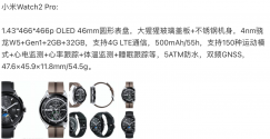
As HW unveiled its product, Xiaomi also unveiled it's watches and wristbands
Please, Log in or Register to view URLs content!

This is what the kirin unveiler said about Xiaomi Watch 2

So again, these higher end watches now seem to all be using Snapdragon W5 SoC. But aside from, they all use OLED screen, support 4G LTE, various sensors, dual band GNSS and probably various other communication protocol.

Just show how much chips get packed into each smart watch. Huge market for domestic supply chain. As Xiaomi looks to develop its own chips, smart wearables seem to be a lower entrance barrier that they can do first before they move into the more demanding phone SoC. Aside from that, no idea how many of the sensors use domestic vs imported supply chain
 

tphuang

Lieutenant General
Staff member
Super Moderator
VIP Professional
Registered Member
Please, Log in or Register to view URLs content!

YMTC showcasing new Ti600 2TB SSD for just 699 RMB.

Using XTacking 3.0 with 7000MB/s read & 6000MB/s write speed

I'm going to guess this is 128 layers, because the read, write & IOPS seem to match the predator GM7 mentioned here
Please, Log in or Register to view URLs content!

Big question for me is where they are in terms of capacity at the moment
 

FairAndUnbiased

Brigadier
Registered Member
Any guess on what the cost split is for a $150 Mn EUV machine in terms of light source to mirror assembly?
Nobody knows without calling Cymer up for a quote but the light source isn't just the Sn droplet chamber, it's everything that goes around it such as the drive laser, droplet generation and targeting capability, ion scavenging mechanism, neutral Sn cleaning, collector mirror, etc.
 

tphuang

Lieutenant General
Staff member
Super Moderator
VIP Professional
Registered Member
Please, Log in or Register to view URLs content!
looks like rockchip's RK3588M auto grade cockpit SoC has more market share than i thought
目前已有多款搭载RK3588M的乘用车面世,仅一年半实现了从产品发布到上车量产,已导入数家国内最具规模的新能源汽车厂商,未来还在导入更多新项目,继续提升汽车电子领域市场份额。
Based on the Antutu report, this 8nm chip is 3rd best SoC tested after SD8295 and SD8195. Better than the more hyped LongYing-1 7nm SoC

除了最具代表性的智能座舱芯片RK3588M,还有仪表盘控制芯片RK3358M、车载音频芯片RK3308M、车载电源管理芯片RK806M、RK809M等
They also have RK3358M for display control, RK3308M for sound control & RK806M/RK809M for PMIC for cars

Please, Log in or Register to view URLs content!
This product was unveiled a year and half ago as being made with 8nm process using QuadCore CPU at 2.1GHz in big core & 1.7GHz in small core supporting 8K display & 7 1080P display output
Comes with 6 TOPS NPU, providing camera inerface
 

dirtyid

New Member
Registered Member

Useful formulas and example parameters set for the design of SSMB storage rings​

A promising accelerator light source mechanism called steady-state microbunching (SSMB) has been actively studied in recent years. Here we summarize some important formulas for the design of SSMB storage rings. Generally we group our formulas into two categories, i.e., a longitudinal weak focusing storage ring for a desired radiation wavelength ≳ 100 nm, and a transverse-longitudinal coupling, or a generalized longitudinal strong focusing, storage ring for a desired radiation wavelength 1 nm ≲ ≲ 100 nm. In each category, we have presented an example parameters set for the corresponding SSMB storage ring, to generate kW-level infrared, EUV and soft X-ray radiation, respectively.

Please, Log in or Register to view URLs content!


Bunch of new papers coming from Tsinghua SSMB in the last few month. Latest first to indicate a lot of technical variables figured out for the design, past conceptual. Focus on many papers seem to focus on transverse-longitudinal coupling variation for 13.5 EUV. This paper was presented late august at the Advanced Beam Dynamics Workshop on Future Light Sources in Switzerland. I don't know implications, but seems there's enough to try move out of concept phase and start building their schematic layouts. Eitherway, the SSMB team is pretty small, same names for the past few years. Plane crash away... one would hope more is going on behind the scenes.

There's also this summary of state of SSMB reserach in Chinese from last year. I'm not great at reading technical Chinese, but it reads optimistic. Pretty similar schematic layout of potential lightsource, but linac power doubled from 400-> 800 MeV in new formula parameters.

Please, Log in or Register to view URLs content!
 

tphuang

Lieutenant General
Staff member
Super Moderator
VIP Professional
Registered Member
Please, Log in or Register to view URLs content!

Jingsheng (crystal growth) believes that it will take 2 more years for 8-inch SiC wafer to be fully in use.
If i had to guess, they would know pretty well when Chinese SiC players turn to 8-inch, so this is likely the timeline. Which if you think about it, is not far off Infineon and ST.

also sounds like it has plenty of orders in its order book and the entire industry is still in explosive growth phase

Please, Log in or Register to view URLs content!
CETC is building a SiC material project in Shanxi
Expecting 300k wafers per year
To start production in 2025
 

tokenanalyst

Brigadier
Registered Member

Sirui Intelligent expands the new track of ion implantation and launches a new dual-track development layout​

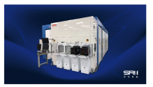
On August 9, the 11th (2023) Semiconductor Equipment Materials and Core Components Exhibition (CSEAC) kicked off at the Wuxi Taihu International Expo Center. 389 domestic and foreign upstream and downstream companies gathered together, covering equipment and key core components. The entire industry chain will jointly create an industry event that integrates industry trends, technology exchanges, demand docking and other dimensions to comprehensively discuss the challenges and opportunities facing the semiconductor industry!

Ion implanters, along with photolithography machines, etching machines and coating equipment, are known as the four core process equipment of chip manufacturing. Currently, ion implantation, as the mainstream technology of doping process, is being widely used in many subdivided fields of semiconductors. The manufacturing of ion implanters not only involves the knowledge of multiple disciplines, but also is the most technically difficult besides photolithography machines. , the front-end process equipment with the lowest localization rate is one of the difficulties that coexists with opportunities and challenges and is waiting to be fully overcome. Qingdao Sifang Sirui Intelligent Technology Co., Ltd. continues to improve its independent innovation capabilities. This year, it launched ion implantation equipment and launched a series of high-energy ion implanters at the CSEAC annual meeting.

1695759946801.png

Please, Log in or Register to view URLs content!
 

TK3600

Major
Registered Member
Do we have any info on performance of chip in Matepad vs Mate 60? Tablet tend to carry better performant chips. These same chips are also used for laptop. It is very relevant these days as some laptop is moving from x86 to arm equivalent, and rely on emulation for legacy software.
 

tokenanalyst

Brigadier
Registered Member

The demand and application of high thermal conductivity silicon carbide ceramics in the semiconductor field​


At present, silicon carbide ( SiC) is a thermally conductive ceramic material that is actively researched at home and abroad. The theoretical thermal conductivity of SiC is very high, with some crystal forms reaching 270W/mK, making it a leader among non-conductive materials. For example, the application of SiC thermal conductivity can be seen in substrate materials for semiconductor devices, high thermal conductivity ceramic materials, heaters and heating plates for semiconductor processing, capsule materials for nuclear fuel, and gas sealing rings for compressor pumps.

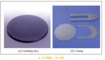
Grinding discs and fixtures are important process equipment for silicon wafer production in the semiconductor industry. If the grinding disc is made of cast iron or carbon steel, its service life will be short and its thermal expansion coefficient will be large. During the processing of silicon wafers, especially during high-speed grinding or polishing, the flatness and flatness of the silicon wafer will deteriorate due to the wear and thermal deformation of the grinding disc. Parallelism is difficult to guarantee. The grinding disc using silicon carbide ceramics has low wear due to its high hardness, and its thermal expansion coefficient is basically the same as that of the silicon wafer, so it can be grinded and polished at high speed.

In addition, when silicon wafers are produced, they need to undergo high-temperature heat treatment. Silicon carbide fixtures are often used for transportation. They are heat-resistant and non-destructive. Coatings such as diamond-like carbon (DLC) can be coated on the surface to enhance performance, alleviate wafer damage, and prevent Contamination spreads.
In addition, as a representative of the third generation of wide bandgap semiconductor materials, silicon carbide single crystal material has a large band gap (about 3 times that of Si), high thermal conductivity (about 3.3 times that of Si or 10 times that of GaAs), Properties such as high electron saturation mobility rate (about 2.5 times that of Si) and high breakdown electric field (about 10 times that of Si or 5 times that of GaAs). SiC devices make up for the shortcomings of traditional semiconductor material devices in practical applications and are gradually becoming the mainstream of power semiconductors.

With the continuous development of science and technology, the demand for silicon carbide ceramics in the semiconductor field has increased rapidly, and high thermal conductivity is a key indicator for its application in semiconductor manufacturing equipment components . Therefore, it is crucial to strengthen the research on high thermal conductivity silicon carbide ceramics. Reducing the oxygen content of the lattice, improving the density, and reasonably regulating the distribution of the second phase in the lattice are the main methods to improve the thermal conductivity of silicon carbide ceramics.
At present, there is little research on high thermal conductivity silicon carbide ceramics in my country, and there is still a large gap compared with the world level. Future research directions include:
Strengthen research on the preparation process of silicon carbide ceramic powder. The preparation of high-purity, low-oxygen silicon carbide powder is the basis for the preparation of high thermal conductivity silicon carbide ceramics;
Strengthen the selection of sintering aids and related theoretical research;
Strengthening the research and development of high-end sintering equipment, and obtaining a reasonable microstructure by regulating the sintering process is a necessary condition for obtaining high thermal conductivity silicon carbide ceramics.
1695761579589.png
Please, Log in or Register to view URLs content!
 
Status
Not open for further replies.
Top