
You are using an out of date browser. It may not display this or other websites correctly.
You should upgrade or use an alternative browser.
You should upgrade or use an alternative browser.
Chinese semiconductor industry
- Thread starter Hendrik_2000
- Start date
- Status
- Not open for further replies.
CXMT was trying to ramp D1x in high volume manufacturing when last Oct's US sanction hit. The sanction was intended to stop CXMT as the cut-off point of 18nm DRAM is basically where CXMT's HVM node is at. The sanction did impact CXMT's plan and all but halted their Fab2 expansion progress.
another article pointing to YMTC fully booked for 6 months next year. I assume this source, but I'd take this as the source being pretty good
Which also to me means YMTC capacity unlikely to change much in first half of next year and that it's growth in Fab 2 most likely start in middle of the year. Maybe it's needs to do more validation of domestic tools + ASML thru the full process.
Now if you remember the AMEC slides, there was more items where DRAMs need customer validation. That to me indicates domestic + ASML to be operational at end of next year. Now, CXMT is not only entity list, so maybe it can still expand a little w/ American tools. Maybe @hvpc can guess us a rough idea here.
And my guess is that 14nm logic using domestic tools + SML gets validated first. It just seems to me that specially for etching tools, the requirement for 1x DRAM is higher than 14nm logic
What I'm now hearing is CXMT has relaxed their D1x (what they called "17nm") design to something a kin to high-18nm-ish DRAM design (i.e. 18.7nm) so it falls just outside of the US's <=18nm sanction cut-off. So CXMT should be able to continue expansion of their revised D1x node wafer capacity.
With high volume manufacturing capacity concerns addressed, CXMT can now focus on technical capability. CXMT can now focus on figuring out to tackle the even more advanced D1z development; they will skip the D1y node.
Since CXMT should now have access to American process equipment for their D1x node, I think they are not pressured to use exclusively domestic process equipment. More likely they continue to accumulate equipment from the western supply chain as their primary tactic while continue to work with Naura/AMEC/etc.. The bar for Naura/AMEC equipment has now gone up...the need is no longer for them to support D1x level performance, now the need is to have them be good enough to support D1z.
Last edited:
Got it. I thought D1x is 19nm, D1y is 17nm & D1z is 15nm? What was their previous D1x & D1y at then? IIRC, I read online they were trying to do D1y DDR5 before sanctions, but did not get the yield up. So, now they won't have DDR5 until D1z? Article I'm referring to.CXMT was trying to ramp D1x in high volume manufacturing when last Oct's US sanction hit. The sanction was intended to stop CXMT as the cut-off point of 18nm DRAM is basically where CXMT's HVM node is at. The sanction did impact CXMT's plan and all but halted their Fab2 expansion progress.
What I'm now hearing is CXMT has relaxed their D1x (what they called "17nm") design to something a kin to high-18nm-ish DRAM design (i.e. 18.7nm) so it falls just outside of the US's <=18nm sanction cut-off. So CXMT should be able to continue expansion of their revised D1x node wafer capacity.
With high volume manufacturing capacity concerns addressed, CXMT can now focus on technical capability. CXMT can now focus on figuring out to tackle the even more advanced D1z development; they will skip the D1y node.
Since CXMT should now have access to American process equipment for their D1x node, I think they are not pressured to use exclusively domestic process equipment. More likely they continue to accumulate equipment from the western supply chain as their primary tactic while continue to work with Naura/AMEC/etc.. The bar for Naura/AMEC equipment has now gone up...the need is no longer for them to support D1x level performance, now the need is to have them be good enough to support D1z.
Micron did D1z and D1a without EUV, right? So theoretically while it may be hard, but D1z with latest DUVi should be doable for CXMT?
Nice I found it
Looks like D1z is a little less than 16nm and both Micron and Samsung were able to do it without EUV. So, CXMT need to basically shrink about 3nm to reach there. Seems like a pretty big jump.
Also from that page, Samsung's D1y was 17.1nm.

Last edited:
wouldn't this Hisilicon chip be an alternative? Am I missing something here?Speaking of projectors, are there domestic alternatives to TI's DMD chips? I assume TI has a big patent wall around it but some important patents must already have expired right? Are DMD chips manufactured in a way similar to normal chips?
wouldn't this Hisilicon chip be an alternative? Am I missing something here?
I assume the Hisilicon chip is a SoC that runs the projector's OS. DMD is the chip in DLP projectors that produces the image. It's basically an array of tiny mirrors that reflects light from the light source.
I see. That seems to be a MEMS chip then. I don't think Hisilicon is working on that type of chip right now. I haven't heard bout either Sai Micro or SMEC fabbing this type of chipI assume the Hisilicon chip is a SoC that runs the projector's OS. DMD is the chip in DLP projectors that produces the image. It's basically an array of tiny mirrors that reflects light from the light source.
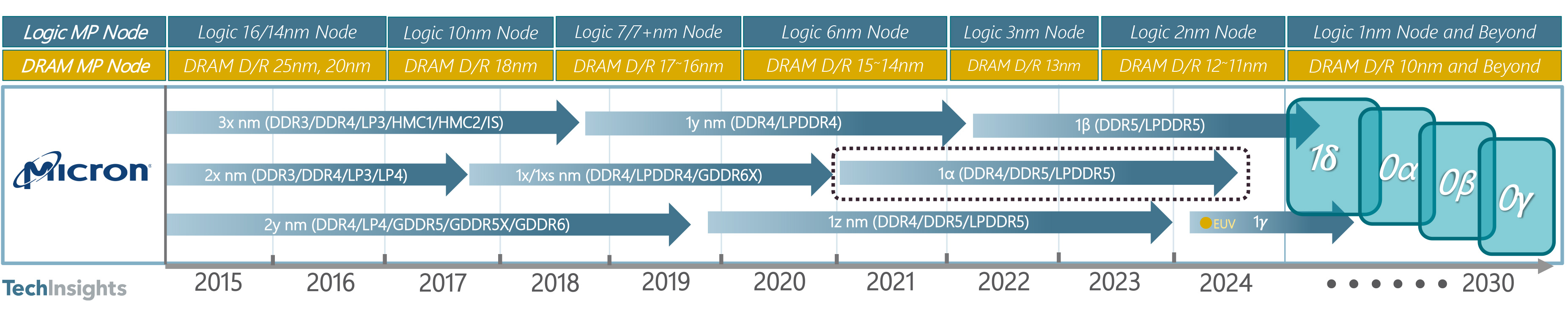
From TechInsights on Micron
Very interesting on this generation comparison bw logic & DRAM
so D1z is essentially comparable to 7+nm
Where as 14nm logic is on comparable to 20nm DRAM
So in my mind, if they could get sub 20nm etching tools validated, then they are already at the N+1 level logic node wise.
+ getting de-americanized 14nm logic line should be easier than getting a de-americanized D1x line
Its seems Huawei Hisilicon unit is recovering in an impressive way...
First the Kirin 9000s, and then its survaillence camera chips:
This report talks as if Huawei manufactures this surveillance chips internally (not sure to interpret this as the "Secret Network for Chips" reported previously by Bloomberg and others... or just bad reporting) in contrast with Kirin 9000s that is fabbed by SMIC.
Im curious where does that chips are fabbed, or if Hisilicon has some kind of manufacturing capabilities for mature nodes.
First the Kirin 9000s, and then its survaillence camera chips:
Im curious where does that chips are fabbed, or if Hisilicon has some kind of manufacturing capabilities for mature nodes.
What I can say is those non-consumer chips came online way before new kirin chips. They just noticed it recently.Its seems Huawei Hisilicon unit is recovering in an impressive way...
First the Kirin 9000s, and then its survaillence camera chips:
This report talks as if Huawei manufactures this surveillance chips internally (not sure to interpret this as the "Secret Network for Chips" reported previously by Bloomberg and others... or just bad reporting) in contrast with Kirin 9000s that is fabbed by SMIC.
Im curious where does that chips are fabbed, or if Hisilicon has manufacturing capabilities.
- Status
- Not open for further replies.