They have a massive FAB in Beijing, so yes you're correct BUT Xian is strategic place, it can create a synergy between Jing-JIN-Ji and Yangtse River Delta Region.Unless they start building fabs then it’s just a different place where they are rumored to open their main office at.
You are using an out of date browser. It may not display this or other websites correctly.
You should upgrade or use an alternative browser.
You should upgrade or use an alternative browser.
Chinese semiconductor industry
- Thread starter Hendrik_2000
- Start date
- Status
- Not open for further replies.
actually, I'm entirely wrong hereSai Micro has started mass production of micro galvanometer which will enable its customer (most likely Robosense here) to make MEMS Lidar
A previous teardown of Robosense Lidar shows that almost all the core chips are sourced from abroad including Micro DRAMs, Xilinx FPGA, chips from TI & analog devices. This is hopefully another step in its way toward establishing domestic supply chain
At the same day that news came out, Ominitron Sensors (a Cali based company) announced that they are using MEMS scanner from Sai Micro/Silex
Now, this does not mean Robosense will not use MEMS scanner from Sai Micro, but I just haven't seen any additional confirmation of that
Another vacuum parts company for semiconductor equipment.
Shanghai Dongbei Vacuum is a high-tech enterprise dedicated to the development, production, sales and service of non-standard complete sets of vacuum equipment. It also has professional equipment such as helium mass spectrometry leak detection, various CNC machine tools, ultra-high vacuum heat treatment furnaces, electrolytic polishing, etc. It also has professional vacuum design, advanced machinery, and electrical engineer service teams to solve system problems in a one-stop manner with a professional perspective. Customer service.
Relying on its strong technical research and development capabilities and service team, the company has achieved a number of scientific research and innovation achievements in the fields of ultra-high and ultra-high vacuum, non-standard complete sets of vacuum application equipment, research on leak detection methods, and reliability traceability standards. It has manufactured a series of high-precision cutting-edge equipment such as vacuum, leakage rate, and material outgassing rate for domestic aviation, aerospace, high-energy physics, universities and other scientific research institutes. The company has successively undertaken and successfully completed the development of national vacuum benchmarks and leakage rate benchmarks. In the field of ultra-high vacuum, it has reached the level of 10-10 Pa, extending the national measurement benchmark. At the same time, the VTL5-10 series of channel-type standard leaks has been developed. This product has reached the international advanced level. It is the only domestic manufacturer that can provide a full range of standard leaks. It has broken the foreign monopoly in this field and has been recognized by relevant experts in the industry.
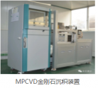
They also develop diamond deposition equipment.

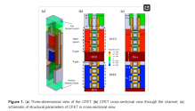
Given what Apple’s new 3 nm processor benchmarks look like I suspect the particulars of transistor design like what we’re seeing in this paper is going to matter more than node sizes for pushing the transistor level performance envelope going forth.
Isn't this just basically going from 2d to 3d? I don't think we need to go to lower node to try going 3d.Given what Apple’s new 3 nm processor benchmarks look like I suspect the particulars of transistor design like what we’re seeing in this paper is going to matter more than node sizes for pushing the transistor level performance envelope going forth.
What do we think about this?
maybe SMIC can try using this Huawei Finfet as an interim step before going to Gaafet. This to me a lot easier to do than Gaa.
FinFET is already 3D. The specific design detail in the paper is about designing a FinFET with a specific cooling feature to improve basic transistor performance.Isn't this just basically going from 2d to 3d? I don't think we need to go to lower node to try going 3d.
What do we think about this?
maybe SMIC can try using this Huawei Finfet as an interim step before going to Gaafet. This to me a lot easier to do than Gaa.
3D stacking of transistors means more heat, reducing gate size could help with thermal issues. The thing that could be accomplish with good deposition and etching tools rather than lithography due the vertical nature of these transistors.Isn't this just basically going from 2d to 3d? I don't think we need to go to lower node to try going 3d.
What do we think about this?
maybe SMIC can try using this Huawei Finfet as an interim step before going to Gaafet. This to me a lot easier to do than Gaa.
that's what I figure. Both etching & deposition seem to be areas where Chinese SMEs are less behind.3D stacking of transistors means more heat, reducing gate size could help with thermal issues. The thing that could be accomplish with good deposition and etching tools rather than lithography due the vertical nature of these transistors.
What I was trying to figure out is what kind of problems you run into if you try GAAFet on 7nm process
- Status
- Not open for further replies.


