Chinese semiconductor industry

Status
Not open for further replies.

tphuang

Lieutenant General
Staff member
Super Moderator
VIP Professional
Registered Member
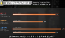
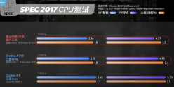
Bro, not sure why you would say that. Below is what Geekerwan shared, it clearly showed Kirin 9000S (red dot) to be below Kirin9000 (yellow line). There are other data like this out there that showed the same.

And in terms of power consumption, the fact that Kirin9000S needs more heat dissipation work-around is almost certainly because 9000S is inferior to Kirin9000 in terms of power consumption/leakage

I'm sure there are other aspects where Kirin9000S may be better due to better chip design optimization. But it is clearly crippled by the fact that it's based on an older technology....there's only so much you can optimize to close the gap with 5nm and Kirin9000, but the lower clock speed, more thermal output is clearly the baggage that comes with using an older tech.
View attachment 118412
Looks like I may have gotten 9000 and SD888 mixed up in my head.

But that still seems to me the difference isn't that large & the A510 power consumption + Taishan medium core power consumption both look fine to me. For regular usage, it's worse than SD8 & Kirin 9000, but nobody will actually be able to tell the difference
Kirin9000S_A510_PowerConsumption.png
TaishanMediumCore_Comparison_PowerConsumption.png

I don't think people are saying that Huawei isn't hamstrung here but that what Hisilicon has designed is good enough that people can still use it as a flagship phone

And this applies to game play people have tested out also.
 

tphuang

Lieutenant General
Staff member
Super Moderator
VIP Professional
Registered Member
so where is this SSA800 being tested?

why do i have a feeling perhaps 'the street' is confused with testing of SMEE's iline system and confused it to be an immersion system?
that's possible. We will find out in due time

that's not possible

Maybe that's why domestic lithography and photoresist stocks are having a field day (basically a whole week's rally).... plus the Huawei announcements
I don't think anyone knows this stuff for sure. There is a lot of speculations in the air these days due to M60.
 

tokenanalyst

Brigadier
Registered Member

500 billion! Suzhou focuses on the development of photonic chips, optical devices, cutting-edge new materials and other fields​


Recently, the Suzhou Municipal People's Government issued the "Opinions on Accelerating the Cultivation of Future Industries" (hereinafter referred to as the "Opinions"). The "Opinions" put forward development goals. By 2030, focus on breakthroughs in a number of key core technologies that fill domestic gaps. Future industries will form effective connections with strategic emerging industries and advantageous leading industries. The city's total future industrial output value will exceed 500 billion yuan.

By 2035, one or two future industrial innovation clusters worth hundreds of billions will be formed, leading the country, and the city's total future industrial output value will exceed 1 trillion yuan.

The "Opinions" clarified the key areas of development, combining the scale advantages of Suzhou's four leading industries of electronic information, equipment manufacturing, biomedicine, and advanced materials, relying on photonics, integrated circuits, artificial intelligence, new energy, innovative drugs, and new nanomaterials We will focus on the development of cutting-edge new materials, photonic chips and optical devices, metaverse, hydrogen energy, digital finance, cell and gene diagnosis and treatment, aerospace development, quantum technology and other future industries.

Among them, in the field of cutting-edge new materials: accelerating the industrialization of cutting-edge new materials such as third-generation semiconductors and other wide-bandgap semiconductor materials, 3D printing and powder metallurgy advanced structural materials, high-performance carbon fibers and composite materials, nanomaterials, and high-temperature superconducting materials. process.

Carry out the preparation of single crystal substrates and epitaxial materials such as silicon carbide (SiC) and gallium nitride (GaN), and promote the research and development and industrialization of key components such as wide bandgap semiconductor power electronic devices and radio frequency devices. Strengthen the construction of public instrument platforms for material synthesis and characterization, and plan and research major projects such as extreme nuclear magnetic resonance and medium-energy multi-particle accelerators. Support scientific research institutions to use materials big data to improve materials genome research capabilities and build a cutting-edge new materials industry innovation system that combines virtualization and experimentation. Encourage all types of innovative entities to target downstream needs such as aerospace, electronic information, energy equipment, life and health, strengthen collaboration in material formulations, synthesis processes, characterization methods, etc., and accelerate technology development in all aspects from material research and development, pilot testing to mass production. breakthrough.
Please, Log in or Register to view URLs content!
 

mrandolph

New Member
Registered Member
How come TechInsights is certain that the Kirin 9000s is made by SMIC?

Is there any kind of technical way to proof this? Or is it just by assumption?

It seems to me a curious gamble for SMIC to play to participate in Huawei's very public endevour. The US could escalate sanctions againt SMIC further using their "foreign direct product rule" forcing ASML and many others to stop supplying them.
 

siegecrossbow

General
Staff member
Super Moderator
How come TechInsights is certain that the Kirin 9000s is made by SMIC?

Is there any kind of technical way to proof this? Or is it just by assumption?

It seems to me a curious gamble for SMIC to play to participate in Huawei's very public endevour. The US could escalate sanctions againt SMIC further using their "foreign direct product rule" forcing ASML and many others to stop supplying them.

Different fabs have different “signatures” unique to the process employed. It is verifiable via microscope analysis.

This is not a gamble when you realize that both Huawei and SMIC have factored in stricter sanctions and concluded that either 1) said sanctions can’t do anything or 2) said sanctions won’t happen.
 

ansy1968

Brigadier
Registered Member
Different fabs have different “signatures” unique to the process employed. It is verifiable via microscope analysis.

This is not a gamble when you realize that both Huawei and SMIC have factored in stricter sanctions and concluded that either 1) said sanctions can’t do anything or 2) said sanctions won’t happen.
Sir from my mentor @Oldschool

Oldschool

Junior Member​

Registered Member
Today at 10:26 PM
Food for thoughts.
Huawei's concurrent 3 new brands , Mate 60 Pro, Mate 60 Pro +, and Mate X5 estimated minimum at 25million units or as much as 200 million units. All 3 brands carry Kirin 9000s 7nm.
That would make us think about SMIC 7nm volume. The previous discussion on this board on SMIC's capacity would not be sufficient.
 

tokenanalyst

Brigadier
Registered Member
so where is this SSA800 being tested?

why do i have a feeling perhaps 'the street' is confused with testing of SMEE's iline system and confused it to be an immersion system?
Well they tested are testing both dry( Arf, I-Line, KrF) and immersion( ArFi), the I-line thing come from a post from a guy in Chinese forum that stated that the I-line was verified by the fabs. The ICRD and SMIC is validating and helping in the developing of the maglev dual wafer stage immersion machine, they working as consortium in which SMIC along side NAURA, SMEE and others are part of and they are investors. To solve problems in the Chinese semiconductor industry, Kind like Sematech.

I Agree that the lithography machine development has been more obscure than other tools maybe to avoid scrutiny from ASML because is going to be really similar.
 

olalavn

Senior Member
Registered Member
This has all the information we want to know (sometimes it's just rumors)

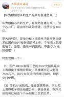
1/Huawei's Kirin chips are produced in Huawei's own chip factory. This chip factory was acquired and built by Huawei with a registered capital of 10 billion
2/ The domestic 28nm process technology DUV lithography machine is independently developed by Shanghai Microelectronics. Multiple exposures can produce 7nm chips. The DUV lithography machine has passed the acceptance and will be delivered soon.
3/

F5WLinFXkAAKns0.jpeg
 

liospopo

New Member
Registered Member
SMSC fab project was announced in 2016. You can look up who the other partners of that JV is

This production line only makes chips for Huawei because Chinese govt is probably telling SMIC you need to support Huawei.

Stop disrespecting other players in the Chinese semiconductor industry.

Hisilicon is clearly the best chip designer in China, but it is just one key part of a large industry

anyways, some interesting stuff about Pro+

DRAM increased to 16GB from 12GB on Pro
Camera improvement also

+the most interesting one for me is the dual support of Tiantong & Beidou 2-way SMS communication. That means the chip tech got even better to support both tiantong satellites and beidou satellites
I am not even talking about SMIC. And it's really not that hard for a company like Huawei to became an IDM.
It‘s not disrespect, it's "Huawei is HUGE, so it must do MORE".
 

bzhong05

New Member
Registered Member
This has all the information we want to know (sometimes it's just rumors)

1/Huawei's Kirin chips are produced in Huawei's own chip factory. This chip factory was acquired and built by Huawei with a registered capital of 10 billion
2/ The domestic 28nm process technology DUV lithography machine is independently developed by Shanghai Microelectronics. Multiple exposures can produce 7nm chips. The DUV lithography machine has passed the acceptance and will be delivered soon.
3/

View attachment 118419
So Huawei has, as a matter of fact, become an IDM?
 
Status
Not open for further replies.
Top