Chinese semiconductor industry

Status
Not open for further replies.

tphuang

Lieutenant General
Staff member
Super Moderator
VIP Professional
Registered Member
Huawei‘s relation to many fabs is quite complicated. Let's say, a chip production line funded by Huawei, and the engineers works on this line also hired by Huawei. And this production line only makes chips for Huawei. Is this Huawei's own production line?Officially, no. So,yeah, Huawei is not fabbing its own chips.:)
SMSC fab project was announced in 2016. You can look up who the other partners of that JV is

This production line only makes chips for Huawei because Chinese govt is probably telling SMIC you need to support Huawei.

Stop disrespecting other players in the Chinese semiconductor industry.

Hisilicon is clearly the best chip designer in China, but it is just one key part of a large industry

anyways, some interesting stuff about Pro+

DRAM increased to 16GB from 12GB on Pro
Camera improvement also

+the most interesting one for me is the dual support of Tiantong & Beidou 2-way SMS communication. That means the chip tech got even better to support both tiantong satellites and beidou satellites
 

hvpc

Junior Member
Registered Member
Eh, I’m going to nitpick a bit more here and point out that you can’t get a clean power consumption and performance comparison simply out of density comparisons. The transistor design itself matters in parameters like voltage swing performance, drive current performance, current leakage, etc. and those are determined by more than feature size measurements.
Indeed, it's more complicated than just simple shrink to obtain the best Power & Performance. Feature size, capacitance, supply voltage, threshold voltage, Gate width, Gate length, etc. all contribute to Power. But in general, smaller feature sizes has a significant influence on the final performance & power consumption, smaller gate width lead to lower threshold voltage and thus lead to lower leakage and thus lower power cosumption.

more than happy to discuss everything in more detail, for example, on why tsmc actually relaxed M1 CD features relative to CPP going from 7nm to 7nm+. What I provided is a general comparison for general consumption for those not intimatly familiar with ins-and-outs of semiconductor design and fabrication.

With that said, actual PPA testing of 7nm, 7nm+, 5nm, 3nm do have the same correlation where the smaller nodes with smaller features have better PPACt performance. And since SMIC basically literally have suspiciously similar process to tsmc, you can assume if it has similar feature dimension it will perform relatively similar to the tsmc one.

Not sure what semiconductor segment you work in, but from a fab process capability standpoint, there is a freakin reason why we track CPP, MMP, cell area, etc.. It's like I said, a general first step of benchmarking that could be done purely on paper. Then subsequent comparison would be to perform actual testing on the actual chip to benchmark PP portion of PPACt. TechInsight does the exact same evaluation, so don't understand what your objection to this methodology is.

If you have data to show larger CPP, M2 transistor have better PPACt do share that data.. Better yet, since you object to the general benchmarking methodology I shared, why don't you show proof that SMIC N+2 with similar feature size to tsmc 7+nm could outperform tsmc 5nm with smaller features or if PPACt performance of nodes with larger featuers would outperform one with smaller featuers?
 

tphuang

Lieutenant General
Staff member
Super Moderator
VIP Professional
Registered Member
I don't think @latenlazy is saying that smaller feature size does not generally result in lower power consumption, but there are other factors involved.

Imo, what matter is the real world data and power consumption of Kirin 9000s seems fine (these are all posted online). Since it's dealing with a clearly less advanced process than Kirin 9000, that's actually quite the credit to Hisilicon team.

We probably will hear more from TechInsight about transistor density on N+2 process. The numbers will probably be close to what you calculated, but we will see. Looks like I jumped the gun in thinking the process is as advanced as N7+ based on the initial performance numbers coming out of the people that tested 9000S.

There is still clearly room for improvement here from SMIC without using EUV. Let's see what they get to for the next gen Kirin chips.

but 1 thing for sure, SMIC & HW seem to have gone all-in together.
 

bzhong05

New Member
Registered Member
Please, Log in or Register to view URLs content!

Anyone paying attention to the recent founding of Shanghai Aishengna (爱晟纳) Electronic Technologies Group? It is co-founded by SMEE's parent company Shanghai Electric with a registered capital of RMB 7 billion and specializes in the manufacturing of semiconductor equipment. Shanghai Electric making a lot of moves recently...
 

hvpc

Junior Member
Registered Member
I don't think @latenlazy is saying that smaller feature size does not generally result in lower power consumption, but there are other factors involved.

Imo, what matter is the real world data and power consumption of Kirin 9000s seems fine (these are all posted online). Since it's dealing with a clearly less advanced process than Kirin 9000, that's actually quite the credit to Hisilicon team.

We probably will hear more from TechInsight about transistor density on N+2 process. The numbers will probably be close to what you calculated, but we will see. Looks like I jumped the gun in thinking the process is as advanced as N7+ based on the initial performance numbers coming out of the people that tested 9000S.

There is still clearly room for improvement here from SMIC without using EUV. Let's see what they get to for the next gen Kirin chips.

but 1 thing for sure, SMIC & HW seem to have gone all-in together.
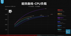
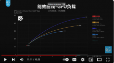
Bro, not sure why you would say that. Below is what Geekerwan shared, it clearly showed Kirin 9000S (red dot) to be below Kirin9000 (yellow line). There are other data like this out there that showed the same.

And in terms of power consumption, the fact that Kirin9000S needs more heat dissipation work-around is almost certainly because 9000S is inferior to Kirin9000 in terms of power consumption/leakage

I'm sure there are other aspects where Kirin9000S may be better due to better chip design optimization. But it is clearly crippled by the fact that it's based on an older technology....there's only so much you can optimize to close the gap with 5nm and Kirin9000, but the lower clock speed, more thermal output is clearly the baggage that comes with using an older tech.
1694183875516.png
1694183965709.png
 

tphuang

Lieutenant General
Staff member
Super Moderator
VIP Professional
Registered Member
Please, Log in or Register to view URLs content!

Anyone paying attention to the recent founding of Shanghai Aishengna (爱晟纳) Electronic Technologies Group? It is co-founded by SMEE's parent company Shanghai Electric with a registered capital of RMB 7 billion and specializes in the manufacturing of semiconductor equipment. Shanghai Electric making a lot of moves recently...
well, the word on the street (not something I got from social media) is that the immersion version of SSA800 has been testing for a while and will be ready for delivery soon.
 

tokenanalyst

Brigadier
Registered Member

Liande Equipment: Preliminarily won the bid for BOE’s high-end module project with a winning price of 490 million yuan​

Liande Equipment announced on the evening of September 8, 2023 that the company was the first winning candidate for BOE's high-end module project, winning the bid for automatic laminating machines and polarizer placement machines, with a winning bid price of 490 million yuan.
Previously, the company received bid winning notices from BOE Chongqing's sixth-generation AMOLED (flexible) display production line twice on February 17 and July 26, 2023. The winning amounts were 85 million yuan and 208 million yuan respectively.
Based on its domestic leading advantages in panel module equipment, Liande Equipment expands into automotive electronics, third-generation semiconductors, and lithium battery equipment to lay a solid foundation for long-term development. The company's main product is semiconductor display automation module equipment, which is used in the middle and rear module assembly processes of flat panel display panels, mainly TFT-LCD, OLED, Mini/MicroLED and other display modules.
The company's product level is domestically leading, and its downstream cooperative customers include panel and consumer electronics companies such as BOE, CSOT, Apple, and Foxconn. Based on the company's advantages in the field of display equipment, the company's module assembly equipment has been successfully expanded into applications in the field of automotive electronics, and has become a supplier of automotive electronics such as Continental Automotive Electronics, Bosch, and Desay SV.
In addition, the company is actively expanding advanced packaging processes such as wafer-level packaging and third-generation semiconductor-related equipment. At the same time, it continues to increase its production of blue films for lithium battery packs, liquid injection machines, cutting and stacking integrated machines, cell assembly and Pack segment complete lines. R&D investment in automation equipment and other equipment.
 

olalavn

Senior Member
Registered Member
Status
Not open for further replies.
Top