ICRD also had one.Huawei has two 1980di.
You are using an out of date browser. It may not display this or other websites correctly.
You should upgrade or use an alternative browser.
You should upgrade or use an alternative browser.
Chinese semiconductor industry
- Thread starter Hendrik_2000
- Start date
- Status
- Not open for further replies.
I thought for sure HLMC got 1980i beforeThe number of advanced lithography machines currently owned in mainland China:
1. 1980i: 6 SMIC South (2018), 6 SMIC Beijing
2. 2000i: 5 SMIC South (2023/7)
3. 2050i: 4 SMIC South (2 in 2021, 2 in 2023/6: 2)
4. Nikon635: 5 sets of ICRD Jiading in the last episode (2022)
View attachment 118292
Something feels off about this.
Now, let's assume this is accurate and they essentially doubled the number of advanced Arfi scanners they have.
If what they had before is sufficient for 35k wpm (8 scanner is probably not enough for that, but I assume they have some 1970i & 1965i also)
then what they have now allows them to get the 35k wpm with SN2
@hvpc does this sound about right to you? Interesting they got that many 2000i
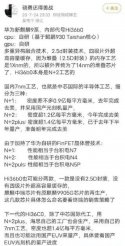
: N+1: The density is about 90 million per square millimeter.
.N+2: The density exceeds 120 million per square millimeter.
N+2plus: The density exceeds 140 million per square millimeter.
Due to the blessing of Huawei’s self-developed FinFET crystal
N+1: Performance equivalent to TSMC N7
N+2: Performance equivalent to TSMC N4
N+2puls: Performance equivalent to TSMC N5P

I thought for sure HLMC got 1980i before
Something feels off about this.
Now, let's assume this is accurate and they essentially doubled the number of advanced Arfi scanners they have.
If what they had before is sufficient for 35k wpm (8 scanner is probably not enough for that, but I assume they have some 1970i & 1965i also)
then what they have now allows them to get the 35k wpm with SN2
@hvpc does this sound about right to you? Interesting they got that many 2000i
@olalavn the date next to the model is the date of delivery or the date of start of production? This is not the same.
These 2 dates are 4/6 months apart and can be very critical especially for the big 5 units of 2000i of July 2023. For installation are mandatory ASML technicians, if machines have been delivered in July then ASML should be allowed to work at SMIC site at least until the end of the year.
Regarding the attached picture, I see 2000i model can be used for 7nm, and 2050i model for 5nm. Considering that SMIC has 4 of them and 2 arrived in June this year (so probably still in installation), it is quite critical 1) the model of the last 3 machines ASML will (hopefully) send within this year 2) to allow ASML technicians to work at SMIC at least until end of the year / early next year.
If everything goes well (this is a big if), SMIC by end 2023 can increase capacity with 2 unit of 2050i (June delivery) + 5 unit of 2000i (July delivery) and by Q1 2024 with the additional 3 units scheduled for delivery this year.
Last edited:
Orient Jingyuan starts listing counseling and plans to IPO on the Science and Technology Innovation Board
On September 5, the China Securities Regulatory Commission issued a report on the guidance and filing of Jingyuan Microelectronics Technology (Beijing) Co., Ltd. Investment Securities Co., Ltd.
According to the data, Dongfang Jingyuan was established in 2014, focusing on the field of integrated circuit manufacturing yield management. At the beginning of its establishment, it established the main direction of attack with electron beam image detection, critical dimension measurement and computational lithography technology. After years of overcoming difficulties, Dongfang Jingyuan has handed over many outstanding report cards. The three core products independently developed by the company, including Computational Lithography Software (OPC), Nanoscale Electron Beam Inspection Equipment (EBI), and 12-inch and 8-inch Critical Dimension Measurement Equipment (CD-SEM), fill a number of gaps in the domestic market.
In 2022, Dongfang Jingyuan will continue to launch a variety of software and hardware products, realize small-scale mass production and repeated orders of many products, and enter a new stage of rapid development.
yes, i saw this online also, but the part about Huwei's Finfet looks to be complete crap, which makes me doubt the other stuff he posted in there.: N+1: The density is about 90 million per square millimeter.
.N+2: The density exceeds 120 million per square millimeter.
N+2plus: The density exceeds 140 million per square millimeter.
Due to the blessing of Huawei’s self-developed FinFET crystal
N+1: Performance equivalent to TSMC N7
N+2: Performance equivalent to TSMC N4
N+2puls: Performance equivalent to TSMC N5P
View attachment 118294
Did they not manage to get any 2100is in?The number of advanced lithography machines currently owned in mainland China:
1. 1980i: 6 SMIC South (2018), 6 SMIC Beijing
2. 2000i: 5 SMIC South (2023/7)
3. 2050i: 4 SMIC South (2 in 2021, 2 in 2023/6: 2)
4. Nikon635: 5 sets of ICRD Jiading in the last episode (2022)
View attachment 118292
That's the delivery date....@olalavn the date next to the model is the date of delivery or the date of start of production? This is not the same.
These 2 dates are 4/6 months apart and can be very critical especially for the big 5 units of 2000i of July 2023. For installation are mandatory ASML technicians, if machines have been delivered in July then ASML should be allowed to work at SMIC site at least until the end of the year.
Regarding the attached picture, I see 2000i model can be used for 7nm, and 2050i model for 5nm. Considering that SMIC has 4 of them and 2 arrived in June this year (so probably still in installation), it is quite critical 1) the model of the last 3 machines ASML will (hopefully) send within this year 2) to allow ASML technicians to work at SMIC at least until end of the year / early next year.
If everything goes well (this is a big if), SMIC by end 2023 can increase capacity with 2 unit of 2050i (June delivery) + 5 unit of 2000i (July delivery) and by Q1 2024 with the additional 3 units scheduled for delivery this year.
Concurrence with @hvpc post about SMIC N+3 performance. So N+2 plus is the pseudo name for 6nm tech and N+3 is for 5nm?: N+1: The density is about 90 million per square millimeter.
.N+2: The density exceeds 120 million per square millimeter.
N+2plus: The density exceeds 140 million per square millimeter.
Due to the blessing of Huawei’s self-developed FinFET crystal
N+1: Performance equivalent to TSMC N7
N+2: Performance equivalent to TSMC N4
N+2puls: Performance equivalent to TSMC N5P
Last edited:
2100 is a DUV model designed specifically for China... replacing EUV... but the U.S. banned it...I guess they discontinued the 2100 model.. EUV is coming soon in China..Did they not manage to get any 2100is in?
- Status
- Not open for further replies.
