Chinese semiconductor industry

Status
Not open for further replies.

PopularScience

Junior Member
Registered Member
Bro for the first time we agree on something....lol My question is how about those technical workers from Taiwan, SK and Japan? will they rather work in China or other places like in the US? I mean with increase compensation plus proximity from home, improve quality of life and cost of living?

Quite alot Koreans working in China semiconductor and LCD industry.
 

tokenanalyst

Brigadier
Registered Member

The total investment is 20 billion! YOFC Advanced Semiconductor's third-generation semiconductor power device R&D and production base settled in Optics Valley​


On August 25, the Management Committee of Wuhan East Lake High-tech Zone and YOFC Advanced Semiconductor Co., Ltd. signed a cooperation agreement on the third-generation semiconductor power device R&D and production base project.

The total investment of the project is expected to exceed 20 billion yuan, of which the total investment of the first phase of the project is 10 billion yuan, which can produce 360,000 SiC MOSFET wafers per year, including epitaxy, device design, wafer manufacturing, packaging, etc.

YOFC Advanced Semiconductor Co., Ltd. focuses on the R&D and manufacturing of silicon carbide (SiC) power semiconductor products. Process production capability and technology research and development capability.

At present, East Lake High-tech Zone focuses on the layout of compound semiconductor industry. Jiufengshan Science and Technology Park will build a whole industrial chain system of equipment, materials, design, chips, devices, modules, manufacturing, packaging and testing, and focus on building a world-class compound semiconductor industry highland.
As one of the four major integrated circuit industry bases in the country, Optics Valley has gathered a group of leading integrated circuit companies at present, forming two major industrial directions of memory chips and compound semiconductor chips, covering design, manufacturing, equipment, materials and distribution, and molds. Groups and other key links in the industrial chain of industrial clusters.

Please, Log in or Register to view URLs content!
 

measuredingabens

Junior Member
Registered Member
The Changchun Institute of Optics and Mechanics has confirmed the acceptance of the first Euv in the second half of the
year.
Unexpectedly, it will be officially delivered to the national team in 2024 at the earliest.

View attachment 117897
Reading the rest of the thread on there, this looks like an interim solution until longer-lasting machines are produced. The approach CIOMP took here is a model that can be made relatively cheaply and have its production rapidly scaled up (at the cost of lifespan and greater power consumption/cooling requirements). It appears to be something to quickly enable more advanced node capacity until more permanent solutions like SSMB come online.
 

tokenanalyst

Brigadier
Registered Member
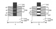
SMIC PMOS AND NMOS GAAFET transistor patent. Deposition is crucial for this kind of devices along with highly selective etching.​

Semiconductor structures and methods of forming them

CN114068700B
Publication Date: 2023-07-28
Filing Date: 2020-06-10
Granted.

Background technique


With the rapid development of semiconductor manufacturing technology, semiconductor transistors are developing towards higher component density and higher integration, and the development trend of semiconductor process nodes following Moore's Law is constantly decreasing. Transistors, as the most basic semiconductor transistors, are currently being widely used. Therefore, with the improvement of component density and integration of semiconductor transistors, in order to adapt to the reduction of process nodes, the channel length of transistors has to be continuously shortened.
In order to better adapt to the scaling down of transistor size, the semiconductor process has gradually begun to transition from planar transistors to three-dimensional transistors with higher efficiency, such as Fin Field Effect Transistors (FinFETs), Fully Surrounded Gates (Gate- all-around, GAA) transistors, etc. Wherein, the all-around gate transistor includes a vertical all-around gate transistor and a horizontal all-around gate transistor. In a fully surrounded gate transistor, the gate surrounds the area where the channel is located. Compared with a planar transistor, the gate of a fully surrounded gate transistor has a stronger ability to control the channel and can better suppress the short channel effect. .
With the further shrinking of the device size, how to achieve a smaller interval between the NMOS device with the fully-enclosed gate structure and the PMOS device with the fully-enclosed gate structure becomes more and more difficult and challenging.

Abstract


A semiconductor structure and its forming method, the forming method comprising: etching the top functional layer and the second functional layer on both sides of the dummy gate of the first region and above the bottom functional layer to form an initial groove; removing the bottom functional layer; Fill sacrificial structures between the second functional layer below the top functional layer and the substrate, between adjacent second functional layers, and remove the second functional layer below the initial groove, or only the second functional layer below the top functional layer Filling the sacrificial structure between the functional layer and the substrate to form a first groove; forming a first source-drain doped layer in the first groove; removing the dummy gate to form a gate opening; removing the sacrificial structure and the second functional layer in the first region forming a first through groove, removing the first functional layer in the second region to form a second through groove; filling the gate opening, the first through groove and the second through groove to form a first device gate and a second device gate. The embodiments of the present invention meet the requirement that different types of fork gate transistors have different numbers of channel layers.


1693407859938.png
 

olalavn

Senior Member
Registered Member
[Huawei provides a solution for the structure and heat dissipation optimization of the chip package pad part]

Example package structure composition

The chip body, multiple conductive pads exposed on the chip surface, and multiple bump structures located on the conductive pads. Each bump structure includes a metal layer and one or more solder caps located on the metal layer.

Technical principles and advantages

Providing multiple welding caps on the metal layer of at least one bump structure can effectively increase the occupied area ratio of the chip bump structure, thereby dispersing the pressure of the bump structure on the inside of the chip during the packaging manufacturing process, and can also increase the bump structure. The heat dissipation capacity and current carrying capacity of the block structure007vgbA7ly1hhf2xd05vqj30xl0aytef.jpg
 

KYli

Brigadier
Copium. It just takes one day for Taiwanese to come up with all these talking points. I have seemed many of these same kinds of comments all over forums in Hong Kong, mainland China and Taiwan.
Please, Log in or Register to view URLs content!
People familiar with the matter answered a series of questions about Huawei's Kirin 9000S mobile processor in a question-and-answer manner.

1. Is this the first time SMIC uses this process technology?

No, SMIC will help a domestic mining machine ship 7nm chips in 2021, and this time it will help Huawei with the same generation (N+2) process technology.

2. Is the Kirin 9000S manufactured using domestic lithography exposure equipment this time?

No, the DUV lithography exposure equipment used by ASML in the Netherlands is the same as the contemporary TSMC lithography exposure equipment, without any localization.

3. Is the Kirin 9000S produced by Huawei's own production line this time?

Totally wrong. Huawei is building its own production line, and even building its own lithography exposure equipment, but these are all very distant things.

At present, Huawei is in the stage of building its own non-beautification production line (that is, the acquisition of Nikon lithography exposure equipment that has been eliminated for many years), and Huawei's self-made lithography exposure equipment is very far away, at least 5 to 10 years before there will be a stage news.

4. Is the Kirin 9000S produced by SMIC's self-built non-beautification production line this time?

No, even if SMIC gets the Nikon lithography exposure equipment, it is impossible to make a 5nm (N+2) chip like the Kirin 9000S. This is an error in the physical principle.

5. Since ASML’s DUV film exposure equipment has been used for a long time, why can SMIC suddenly manufacture Kirin 9000S for Huawei?

Because this year, Biden and the White House Department of Commerce made a decision to allow SMIC to provide a license to manufacture 5nm chips for Huawei.

According to previous media reports, sufficient production capacity and stocking will be achieved by the end of this year. However, when the yield rate was low and the output was insufficient, Huawei directly produced mobile phones and released them offline, which caused today's shock.

6. Can SMIC continue to make breakthroughs in process technology and carry out 4nm-level chip foundry?

It is impossible at present, because it is necessary to purchase a large amount of ASML's EUV shadow exposure equipment, but at present, the sale of this shadow exposure equipment is completely banned by SMIC, so the current Kirin 9000S is what SMIC can achieve in the next 5 to 10 years. the best process technology.

Unless SMIC is lifted the ban on EUV shadow exposure equipment, or the White House licenses ASML to sell EUV shadow exposure equipment to SMIC, SMIC can only optimize "N+3", "N+4" and so on on the current basis.

7. Does Shanghai Microelectronics (SMEE) have the opportunity to develop EUV shadow exposure equipment?

impossible.

8. Will ASML sell photo exposure equipment to Huawei's self-built production line?

impossible.

9. Are there any other de-beautification solutions to help Huawei OEM?

Likelihood is 0.
 

liospopo

New Member
Registered Member
Copium. It just takes one day for Taiwanese to come up with all these talking points. I have seemed many of these same kinds of comments all over forums in Hong Kong, mainland China and Taiwan.
Please, Log in or Register to view URLs content!
People familiar with the matter answered a series of questions about Huawei's Kirin 9000S mobile processor in a question-and-answer manner.

1. Is this the first time SMIC uses this process technology?

No, SMIC will help a domestic mining machine ship 7nm chips in 2021, and this time it will help Huawei with the same generation (N+2) process technology.

2. Is the Kirin 9000S manufactured using domestic lithography exposure equipment this time?

No, the DUV lithography exposure equipment used by ASML in the Netherlands is the same as the contemporary TSMC lithography exposure equipment, without any localization.

3. Is the Kirin 9000S produced by Huawei's own production line this time?

Totally wrong. Huawei is building its own production line, and even building its own lithography exposure equipment, but these are all very distant things.

At present, Huawei is in the stage of building its own non-beautification production line (that is, the acquisition of Nikon lithography exposure equipment that has been eliminated for many years), and Huawei's self-made lithography exposure equipment is very far away, at least 5 to 10 years before there will be a stage news.

4. Is the Kirin 9000S produced by SMIC's self-built non-beautification production line this time?

No, even if SMIC gets the Nikon lithography exposure equipment, it is impossible to make a 5nm (N+2) chip like the Kirin 9000S. This is an error in the physical principle.

5. Since ASML’s DUV film exposure equipment has been used for a long time, why can SMIC suddenly manufacture Kirin 9000S for Huawei?

Because this year, Biden and the White House Department of Commerce made a decision to allow SMIC to provide a license to manufacture 5nm chips for Huawei.

According to previous media reports, sufficient production capacity and stocking will be achieved by the end of this year. However, when the yield rate was low and the output was insufficient, Huawei directly produced mobile phones and released them offline, which caused today's shock.

6. Can SMIC continue to make breakthroughs in process technology and carry out 4nm-level chip foundry?

It is impossible at present, because it is necessary to purchase a large amount of ASML's EUV shadow exposure equipment, but at present, the sale of this shadow exposure equipment is completely banned by SMIC, so the current Kirin 9000S is what SMIC can achieve in the next 5 to 10 years. the best process technology.

Unless SMIC is lifted the ban on EUV shadow exposure equipment, or the White House licenses ASML to sell EUV shadow exposure equipment to SMIC, SMIC can only optimize "N+3", "N+4" and so on on the current basis.

7. Does Shanghai Microelectronics (SMEE) have the opportunity to develop EUV shadow exposure equipment?

impossible.

8. Will ASML sell photo exposure equipment to Huawei's self-built production line?

impossible.

9. Are there any other de-beautification solutions to help Huawei OEM?

Likelihood is 0.
Lol, this level of copium.
 

BlackWindMnt

Captain
Registered Member
Copium. It just takes one day for Taiwanese to come up with all these talking points. I have seemed many of these same kinds of comments all over forums in Hong Kong, mainland China and Taiwan.
Please, Log in or Register to view URLs content!
People familiar with the matter answered a series of questions about Huawei's Kirin 9000S mobile processor in a question-and-answer manner.

1. Is this the first time SMIC uses this process technology?

No, SMIC will help a domestic mining machine ship 7nm chips in 2021, and this time it will help Huawei with the same generation (N+2) process technology.

2. Is the Kirin 9000S manufactured using domestic lithography exposure equipment this time?

No, the DUV lithography exposure equipment used by ASML in the Netherlands is the same as the contemporary TSMC lithography exposure equipment, without any localization.

3. Is the Kirin 9000S produced by Huawei's own production line this time?

Totally wrong. Huawei is building its own production line, and even building its own lithography exposure equipment, but these are all very distant things.

At present, Huawei is in the stage of building its own non-beautification production line (that is, the acquisition of Nikon lithography exposure equipment that has been eliminated for many years), and Huawei's self-made lithography exposure equipment is very far away, at least 5 to 10 years before there will be a stage news.

4. Is the Kirin 9000S produced by SMIC's self-built non-beautification production line this time?

No, even if SMIC gets the Nikon lithography exposure equipment, it is impossible to make a 5nm (N+2) chip like the Kirin 9000S. This is an error in the physical principle.

5. Since ASML’s DUV film exposure equipment has been used for a long time, why can SMIC suddenly manufacture Kirin 9000S for Huawei?

Because this year, Biden and the White House Department of Commerce made a decision to allow SMIC to provide a license to manufacture 5nm chips for Huawei.

According to previous media reports, sufficient production capacity and stocking will be achieved by the end of this year. However, when the yield rate was low and the output was insufficient, Huawei directly produced mobile phones and released them offline, which caused today's shock.

6. Can SMIC continue to make breakthroughs in process technology and carry out 4nm-level chip foundry?

It is impossible at present, because it is necessary to purchase a large amount of ASML's EUV shadow exposure equipment, but at present, the sale of this shadow exposure equipment is completely banned by SMIC, so the current Kirin 9000S is what SMIC can achieve in the next 5 to 10 years. the best process technology.

Unless SMIC is lifted the ban on EUV shadow exposure equipment, or the White House licenses ASML to sell EUV shadow exposure equipment to SMIC, SMIC can only optimize "N+3", "N+4" and so on on the current basis.

7. Does Shanghai Microelectronics (SMEE) have the opportunity to develop EUV shadow exposure equipment?

impossible.

8. Will ASML sell photo exposure equipment to Huawei's self-built production line?

impossible.

9. Are there any other de-beautification solutions to help Huawei OEM?

Likelihood is 0.
Is Beautification a miss translation of 美国?
 
Status
Not open for further replies.
Top