Maybe this would finally have a chilly effect and prompt Chinese domestic firms to accelerate adoption of Chinese alternatives. It could also open up Middle East market for Chinese semiconductor firms as the US expands the restrictions of high tech to more countries.
You are using an out of date browser. It may not display this or other websites correctly.
You should upgrade or use an alternative browser.
You should upgrade or use an alternative browser.
Chinese semiconductor industry
- Thread starter Hendrik_2000
- Start date
- Status
- Not open for further replies.
Truly a gift that keeps on giving. This basically cedes the Middle East market to China since Chinese Atlas 900 clusters can rival A100's and H100 (??) from Nvidia. Can someone confirm the H100 bit?Maybe this would finally have a chilly effect and prompt Chinese domestic firms to accelerate adoption of Chinese alternatives. It could also open up Middle East market for Chinese semiconductor firms as the US expands the restrictions of high tech to more countries.
Don't these idiots know you don't need bleeding edge nodes to make top tier AI GPUs? Don't interrupt the enemy while they are making a mistake! More AI sanctions, the better. This will give domestic companies only one choice (national resiliency) instead of pure economic motivations.
Wuxi Innolux's third-generation semiconductor module packaging and testing project is planned to be put into production at the end of December
Recently, new progress has been made in the third-generation semiconductor module packaging and testing project of Innolux located in Xishan Economic and Technological Development Zone, Wuxi, and the remanufacturing project of Kaiwites semiconductor equipment parts.
According to news from Xishan Economic and Technological Development Zone, the main body of the third-generation semiconductor module packaging and testing project of Innosilicon is capped, and the civil construction is planned to be completed in October and put into production at the end of December; The roof is capped, and the civil works are planned to be completed in December and put into operation in March 2024.
It is reported that the third-generation semiconductor module packaging and testing project of Innosilicon has a total investment of 800 million yuan, with a land area of 27 mu and a construction area of 31,000 square meters. It will build a project with an annual output of 1.2 million automotive-grade power device modules, and its products cover power semiconductor modules. , discrete devices, etc., mainly used in new energy vehicles, new energy green electricity, charging piles, energy storage and other fields.
Kaiwites semiconductor equipment parts remanufacturing project covers an area of about 50 acres and a construction area of about 50,000 square meters. It is mainly engaged in the remanufacturing of semiconductor equipment parts and core parts manufacturing. After the project is put into operation, it will produce 200,000 sets of semiconductor spare parts and clean 400,000 sets of semiconductor spare parts annually.
Truly a gift that keeps on giving. This basically cedes the Middle East market to China since Chinese Atlas 900 clusters can rival A100's and H100 (??) from Nvidia. Can someone confirm the H100 bit?
Don't these idiots know you don't need bleeding edge nodes to make top tier AI GPUs? Don't interrupt the enemy while they are making a mistake! More AI sanctions, the better. This will give domestic companies only one choice (national resiliency) instead of pure economic motivations.
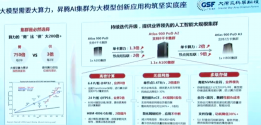
you mean like this one? The Atlas 900 PoD A3?
It actually might be easier to get Middle Eastern customers hooked onto Huawei products than some of HW's competitors since they don't already have something fully built into their system of using A100
Han's Semiconductor: High-end wafer laser cutting equipment achieves a breakthrough in 100% localization of core components
Recently, Shenzhen Han's Semiconductor Equipment Technology Co., Ltd. ("Han's Semiconductor"), a wholly-owned subsidiary of Han's Laser, has developed a high-end wafer laser cutting equipment with 100% localization of core components by virtue of its rich experience in industry technology development and process application. ——Han's Semiconductor DA100 laser cutting system (hereinafter referred to as "DA100") has filled the technical gap in the field of semiconductor wafer cutting in my country and successfully broken the foreign monopoly.
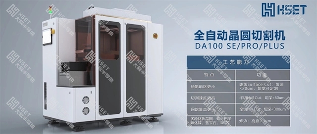
Han’s Semiconductor DA100 is a system for cutting and separating wafers based on the Ablation process principle. This series of equipment is a high-compatibility laser surface cutting system optimized and developed for different characteristics of multiple industries. It can freely cut the front and back sides of different tracks and multiple products. , to achieve the highest precision in the industry. At the same time, on the basis of the original cutting materials, technological breakthroughs in processing silicon, gallium arsenide, gallium nitride, sapphire, indium phosphide, ceramics, metals and other materials have been realized, which is the development process of Han's semiconductor laser processing equipment an important milestone in .
Han’s Semiconductor DA100 can meet the cutting needs of various types of wafers, and can perform surface cutting (cutting depth ≤ 20 μm, cutting width can be customized), half cutting (cutting depth ≤ 100 μm, cutting width ≤ 20 μm) and full cutting (cutting depth ≤200μm, cutting width ≤30μm) three separation processes, functions can be configured on demand to provide customized services, further reducing the cost of use for customers.
On the H100, China will probably need EUV to match it (although it might be able to by pushing DUVi down to 5nm). We've just heard that CIOMP has an EUV prototype (or will in the second half of the year, so either now or within the next 4 months), and I expect that the first commercial machines (or even advanced prototypes) will be fabbing GPGPUs from Biren and the like given their strategic importance.Truly the gift that keeps on giving. This basically cedes the Middle East market to China since Chinese Atlas 900 clusters can rival A100's and H100 (??) from Nvidia. Can someone confirm the H100 bit?
Don't these idiots know you don't need bleeding edge nodes to make top tier AI GPUs? Don't interrupt the enemy while they are making a mistake! More AI sanctions, the better. This will give domestic companies only one choice (national resiliency) instead of pure economic motivations.
Nvidia: "Help. I cannot breath". #NvidiaLifeMatters.Truly a gift that keeps on giving. This basically cedes the Middle East market to China since Chinese Atlas 900 clusters can rival A100's and H100 (??) from Nvidia. Can someone confirm the H100 bit?
Don't these idiots know you don't need bleeding edge nodes to make top tier AI GPUs? Don't interrupt the enemy while they are making a mistake! More AI sanctions, the better. This will give domestic companies only one choice (national resiliency) instead of pure economic motivations.
Sudaweige's high-performance lithography equipment was successfully delivered: helping the development and innovation of photonic chips, optical communications and other optoelectronic industries!
Recently, the large-scale direct writing lithography equipment independently developed and manufactured by Sudaweige was successfully delivered. This equipment is mainly used for photolithography manufacturing of photonic chips, optical communications and optical chips and other related materials in the field of optoelectronics, and builds a high-end equipment platform for the manufacture of advanced optoelectronic devices for customers.With the acceleration of the intelligent process of various industries and the explosion of data traffic, chips, devices and related modules in the field of optoelectronics are evolving towards high speed, integration, large capacity, and low cost, which is the industrial expansion of the company's high-performance lithography equipment bring great opportunities.
The large-scale direct writing lithography equipment independently developed by Sudaweige has comprehensive performance advantages:
-Transformation of 3D vector design data into microstructure topography with advanced algorithms and software processing
-Mass data processing and transmission/fast lithography
-Large-area substrate real-time three-dimensional navigation self-focusing function
-Proximity Effect Compensation for Exposure of 3D Microstructure Topography
-Support the preparation of large-area lithography thick plastic sheet…
It can provide key technical support and high-end manufacturing platform for the manufacturing and industrial innovation of various novel optoelectronic materials and related functional devices.
At present, Sudaweige has signed several large-scale lithography equipment contracts, which are mainly used for lithography processing and production of related materials and devices in the fields of photonic chips, optical chips, photomasks, bill anti-counterfeiting, pan-semiconductors, etc. The company will continue to follow relevant agreements deliver.
Sudaweige will continue to expand micro-nano optical technology/products in national bills and certificate anti-counterfeiting materials, electronic paper and reflective liquid crystal front light materials, AR/MR and AR-HUD diffractive optical materials, chip photolithography machine positioning grating ruler materials, and the commercial application and industrialization investment of lithography equipment in photovoltaic copper electroplating patterning equipment, high-end masks, photonic chips, optical chips and other fields with higher added value and market space, strives to provide customers with advanced optical materials, lithography Equipment and solutions to meet customers' higher demand for micro-nano lithography manufacturing, help them break through technical bottlenecks, and create new opportunities for industrial cooperation.
Su Daweige said on the interactive platform that lithography equipment is the company's key business expansion area. This year, the company's orders for various lithography equipment have increased significantly year-on-year, driving equipment sales revenue to increase by about 950% year-on-year in the first half of the year. The lithography equipment sold by the company to relevant top customers can be used for the production of masks and other devices.
Me too, I've been tempered by our esteem colleague to deflate my expectation, now I regret it....lolPlease don't go China speed or else I'm losing my bet about EUV in 2025, while China on China speed will release EUV in 2024
Huahai Zero2IPO (688120): 23H1 revenue and profit increased year-on-year with high growth, new generation of CMP, thinning and other new products accelerated verification
Huahai Qingke released the 2023 semi-annual report, with revenue of 1.23 billion yuan, +72% year-on-year, and non-net profit of 307 million yuan, +114% year-on-year. The company's revenue and profit have grown rapidly year-on-year, and new product verification is progressing smoothly.
In 23H1, revenue and profit grew rapidly year-on-year. 23H1 revenue was 1.234 billion yuan, +72% year-on-year; net profit attributable to the parent was 374 million yuan, +101% year-on-year; net profit not attributable to the parent was 307 million yuan, +114% year-on-year.
In 23Q2, the revenue grew rapidly year-on-year, and the gross profit margin was stable. 23Q2 revenue was 620 million yuan, +68% year-on-year/+0.3% quarter-on-quarter; gross profit margin was 46%, -0.8pct year-on-year/-0.7pct quarter-on-quarter; net profit attributable to the parent was 180 million yuan, +91% year-on-year/-7% quarter-on-quarter; The net profit not attributable to the parent company was 140 million yuan, +113% year-on-year/-16% month-on-month; non-net profit rate was 22.7%, +4.8pcts year-on-year/-4.4pcts month-on-month.
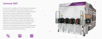
The H300 machine has completed the basic process performance verification, and the thinning and polishing all-in-one machine has been sent to a leading IC company for verification.
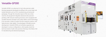
The company launched the Universal H300 machine, which optimizes the cleaning technology module and has completed product development and basic process performance verification; the Universal-150 Smart for the third-generation semiconductor is compatible with polishing various semiconductor materials of 6-8 inches, and has four independent polishing units , to meet the third-generation semiconductor, MEMS, etc., and has been sent to two third-generation semiconductor customers for verification; advanced packaging and large silicon wafer CMP are delivered to customers' large production lines in batches; compound-oriented equipment is applied in SiC, GaN, LN, LT, etc. Obtained batch orders; Versatile-GP300 thinning and polishing all-in-one machine is used for front-end wafer back thinning. The mass-produced machine has been sent to leading IC companies for verification, and its performance has been recognized by customers; it is applied to Cu, Al, W, Co and other metals The film thickness measurement equipment FTM-M300 of the process has been sent to many customers for verification, and small batch shipments have been realized.
The wafer regeneration capacity reached 100,000 pieces/month, and the diversified verification of the 7-zone polishing head was successfully promoted to major customers. The wafer regeneration capacity has reached 100,000 pieces/month, and all the isolation work of the two production lines of Cu/Non Cu in the factory area has been completed; the demo verification work has been completed in well-known domestic manufacturers, and batch orders have been obtained from many large production lines to achieve long-term stable supply. In the maintenance business of consumables, the diversified verification of polishing heads in the 7th area has been successfully promoted to large customers. With the continuous increase in the number of CMP equipment, maintenance of consumables will become a new growth point for the company's future profits.
- Status
- Not open for further replies.

