Chinese semiconductor industry

Status
Not open for further replies.

tokenanalyst

Brigadier
Registered Member
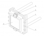
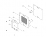
This is the patent for the above module, different from using a mercury lamp this UV light source looks pretty compact for the power.

A light source head assembly of a lithography machine
App Num:
CN202310743157.2
File Date:
2023-06-21
Pub Num:
CN116520650A
Publish Date:
2023-08-01
Assignee:
Zhangjiagang Qidian Photoelectric Technology Co., Ltd.
Abstract
The present invention relates to the technical field of photolithography machine light source components, in particular to a photolithography machine light source head assembly, including a light source device, a collimation module, an air cooling device and a water cooling device. The rear of the light source device is fixedly connected to the water cooling device. An air-cooling device is provided in the light source device, and a collimation module is provided on one side of the light source device. The light source device includes a rear plate, an engaging body and a clamping device. , the front plate is provided with evenly distributed bolts. In the present invention, through the fixed block, the connecting rod, the engaging rod, the mounting block, the chute, the fixing plate, the positioning rod, the first spring and the clamping body , you can directly push the clamping rod, and push the clamping body to move through the clamping rod. After the bottom of the clamping rod contacts the mounting block, release the clamping rod, and the clamping body can engage the clamping body under the action of the first spring. The rod is engaged, and the engaging rod is pushed to move at the same time, so as to realize the fast installation of the fixed shell.​

1691531981916.png1691532036671.png
 

FairAndUnbiased

Brigadier
Registered Member
Interesting company entering the field of LED UV lithography, pretty high power UVLED light sources. Hopefully they could supply to SMEE in the future.

Zhangjiagang Qidian Optoelectronics Technology Co., Ltd. is a high-tech enterprise in the field of optoelectronics jointly funded by the Chongqing Institute of Green and Intelligent Technology of the Chinese Academy of Sciences, the Zhangjiagang government and the scientific research team of the Chinese Academy of Sciences. Innovative technology is applied to exposure machine equipment to produce the world's leading UVLED exposure machine module products. The application of this product in the PCB printed circuit board industry has broken the monopoly of high-end exposure equipment by Europe and Japan. The company is further expanding its business field, entering the field of LCD liquid crystal panels and even the field of semiconductor integrated circuits in five years, and

View attachment 116970View attachment 116971

Please, Log in or Register to view URLs content!
I've been talking about UV LED lithography for a while. The vast cost and energy savings from LED lithography is enough to absolutely cabbagize display and chiplet markets.

Mercury lamps used in current i-line lithography go bad after 1-2 months, are like 5% energy efficient and create hazardous mercury waste.

365 nm UV LEDs are 50% energy efficient and last 50k hours of use (staying on for 6 years continuously). They create regular e waste which is dangerous but not as bad as mercury.
 

tphuang

Lieutenant General
Staff member
Super Moderator
VIP Professional
Registered Member
That is the real message.

Huawei has left Quaalcom.

Is anyone next?

I would say to hold it on the over excitement. The moment that Huawei produces a competitive flagship 5g phone without American mobile rf component would be a shock for this industry. Even so, other mobile phone makers in china don't have same urgent need to de Americanize. As such, they can continue their pace of gradually on boarding domestic rf fe chips.

Let's say Huawei 5g phone is a great success, there are still some real questions.

How many 5g modems can be fabbed by smic? Let's say hisilicon found an advanced packaging for 5g modem that allows it to be manufactured with 12nm process. Guess what? Smic still has limited 12nm capacity. Smartphones are sold in the hundreds of millions a year. How many 12nm wafers would be needed to cover 100 million phones 5g modem. I haven't done the calculations, but would assume a pretty large number. So they need to ramp up 12/14nm capacity first

Aside from that, a 5g phone requires 70 to 100 rf filters as well as many other components and integrated modules. How much mems capacity does china currently have. How long will it take to ramp up what's needed for 100 million phones?

Remember, Huawei itself will probably want to manufacture 60 million phones next year. How many do you think all the other major Chinese phone makers need?

The market for smic and smec is huge but so is the task to ramp up that production.

On top of phones, there are more modems, socs, rf components needed for tablets, laptops, cars, wearables and other iot devices.

You don't think Huawei is going to build an OS for IoT world and cultivate a domestic supply chain without first feeding itself, do you?
 

tokenanalyst

Brigadier
Registered Member
I've been talking about UV LED lithography for a while. The vast cost and energy savings from LED lithography is enough to absolutely cabbagize display and chiplet markets.

Mercury lamps used in current i-line lithography go bad after 1-2 months, are like 5% energy efficient and create hazardous mercury waste.

365 nm UV LEDs are 50% energy efficient and last 50k hours of use (staying on for 6 years continuously). They create regular e waste which is dangerous but not as bad as mercury.
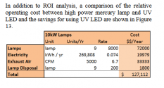
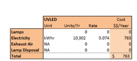
According to onto the savings are huge.
1691535612669.pngVS 1691535639754.png

Please, Log in or Register to view URLs content!

Also mercury lamps need hefty electric circuitry, optical filtering, focusing and homogenization so there could be a reduction in machine production costs apart form usage cost.
 

tinrobert

Junior Member
Registered Member
wow... Apple is making it difficult for TSMC...
Please, Log in or Register to view URLs content!
Totally unsubstantiated. The article was based on a report provided to EE Times by Brett Simpson, senior analyst at Arete Research, who said”

“We think TSMC will move to normal wafer-based pricing on N3 with Apple during the first half of 2024, at around $16-17K average selling prices. At present, we believe N3 yields at TSMC for A17 and M3 processors are at around 55% [a healthy level at this stage in N3 development], and TSMC looks on schedule to boost yields by around 5+ points each quarter.”

I bolded the words "think" and "believe". Nothing mentioned in TSMC's 20-F or earnings call on this.
 

tinrobert

Junior Member
Registered Member
According to onto the savings are huge.
View attachment 116974VS View attachment 116975

Please, Log in or Register to view URLs content!

Also mercury lamps need hefty electric circuitry, optical filtering, focusing and homogenization so there could be a reduction in machine production costs apart form usage cost.
This article was written in 2006 before Rudolph merged with Nanometrics to form Onto. Both were started as metrology/inspection companies but couldn't compete with KLA. They merged and still can't move the needle, and so they are moving to a packaging equipment company with less competition.
 

huemens

Junior Member
Registered Member
I would say to hold it on the over excitement. The moment that Huawei produces a competitive flagship 5g phone without American mobile rf component would be a shock for this industry. Even so, other mobile phone makers in china don't have same urgent need to de Americanize. As such, they can continue their pace of gradually on boarding domestic rf fe chips.

Let's say Huawei 5g phone is a great success, there are still some real questions.

How many 5g modems can be fabbed by smic? Let's say hisilicon found an advanced packaging for 5g modem that allows it to be manufactured with 12nm process. Guess what? Smic still has limited 12nm capacity. Smartphones are sold in the hundreds of millions a year. How many 12nm wafers would be needed to cover 100 million phones 5g modem. I haven't done the calculations, but would assume a pretty large number. So they need to ramp up 12/14nm capacity first

Aside from that, a 5g phone requires 70 to 100 rf filters as well as many other components and integrated modules. How much mems capacity does china currently have. How long will it take to ramp up what's needed for 100 million phones?

Remember, Huawei itself will probably want to manufacture 60 million phones next year. How many do you think all the other major Chinese phone makers need?

The market for smic and smec is huge but so is the task to ramp up that production.

On top of phones, there are more modems, socs, rf components needed for tablets, laptops, cars, wearables and other iot devices.

You don't think Huawei is going to build an OS for IoT world and cultivate a domestic supply chain without first feeding itself, do you?

Here's some numbers for the early Huawei 5G modem.
The first huawei 5G phone used a standalone Balong 5G modem (it combines support for 2G, 3G, 4G and 5G). The die size of that modem was 9.82mm x 8.74mm. It was fabbed on TSMC 7FF.

When Kirin 990 5G SoC came out modem was integrated into it. The combined die size of Kirin 990 with integrated modem was 10.68mm x 10.61mm. So modem design must have been significantly optimized by the time of Kirin 990.

About RF components, first 5G phone used RF components from US companies. The next Mate device was de-americanized and used RF components from a Japanese company.
 

FairAndUnbiased

Brigadier
Registered Member
According to onto the savings are huge.
View attachment 116974VS View attachment 116975

Please, Log in or Register to view URLs content!

Also mercury lamps need hefty electric circuitry, optical filtering, focusing and homogenization so there could be a reduction in machine production costs apart form usage cost.
The fact that it was not ASML that caught this, and instead still sell i-line lithography with mercury lamps, and has no sign of even attempting UV-LED lithography, says volumes.
This article was written in 2006 before Rudolph merged with Nanometrics to form Onto. Both were started as metrology/inspection companies but couldn't compete with KLA. They merged and still can't move the needle, and so they are moving to a packaging equipment company with less competition.
that does not mean UVLED lithography is a bad idea for substituting i-line. As you know, lithography tools for legacy nodes are hard to make too much money from, as new build tools from incumbents are already pretty cheap, and new build, new tech tools have to compete with used tools that are more familiar from suppliers that are already preferred to fabs.

smaller companies are often forced to be more innovative to survive in markets with lower profit margins like packaging, display, etc than big companies with subsidies that get on the IRDS.

Please, Log in or Register to view URLs content!

UV LED light source tech is already surpassing mercury in intensity, so its not a technical limitation.

Please, Log in or Register to view URLs content!
 
Status
Not open for further replies.
Top