Chinese semiconductor industry

Status
Not open for further replies.

tphuang

Lieutenant General
Staff member
Super Moderator
VIP Professional
Registered Member
Here's some numbers for the early Huawei 5G modem.
The first huawei 5G phone used a standalone Balong 5G modem (it combines support for 2G, 3G, 4G and 5G). The die size of that modem was 9.82mm x 8.74mm. It was fabbed on TSMC 7FF.

When Kirin 990 5G SoC came out modem was integrated into it. The combined die size of Kirin 990 with integrated modem was 10.68mm x 10.61mm. So modem design must have been significantly optimized by the time of Kirin 990.

About RF components, first 5G phone used RF components from US companies. The next Mate device was de-americanized and used RF components from a Japanese company.

I have posted teardown board of a phone here where you can see how much rf components and 5g modem take up large chunk of real estate.

5g modem and soc are not the same thing. They can be tightly integrated but each have their own space on the board.

Eg with Qualcomm, you had x50 and then 55. Now believe they are on x70. For Huawei phone, the 5g chip set will likely be stacked 14nm does and soc likely stacked 7nm. Also consider that stacking 2 dies mean combined size probably 2x die size of a 5nm process soc. Necessary for achieving comparable performance. Think about why Intel CPUs are always so much larger than AMD ones.

But due to the less advanced process for both AOC and modem, Huawei phones need latest heat dissipation tech + more advanced battery tech to achieve comparable performance.

Anyways, let's say all this is resolved for Huawei's mid ranged phones using kirin chip, we now have a fully sanction proof 5g phone. That's quite the accomplishment.

As for 5g components, you are entirely wrong here. A tear down of mate 40 would proof that. So yes, they did use more stuff from Murata, but still a whole lot of of qualcomm, qorvo & skyworks
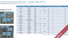
HW_Mate50_RFFE_Suppliers.JPG
 

huemens

Junior Member
Registered Member
5g modem and soc are not the same thing. They can be tightly integrated but each have their own space on the board.
It goes both ways. Even Qualcomm sell some SoC with builtin modem. They can either include the modem as part of the SoC or supply as a separate module. As I said in my post Huawei used 5G modem as a separate module on Mate 20x 5G, because the SoC it used was Kirin 980, which already had a 4G modem baked into it. Therefore that phone technically had two modems but only the external 5G one was used.
But when they released Mate 30 they had incorporated the 5G modem directly into the Kirin 990 SoC, similar to the way they had a 4G modem in the Kirin 980. You can check the board of that phone and see there is no extra modem. Not only that they also stacked the RAM on top of the SoC. So on that phone for real estate purposes the SoC + Modem + RAM is occupying a single space.

As for 5g components, you are entirely wrong here. A tear down of mate 40 would proof that. So yes, they did use more stuff from Murata, but still a whole lot of of qualcomm, qorvo & skyworks
Here also I was specifically talking about Mate 30. In that they did not use American RF. My point was to say that it was doable without American RF even 4 years ago. And I think Huawei's point was also to demonstrate that it is doable, because they re-introduced American parts in Mate 30 pro.

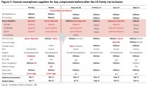
Here is a comparison of parts suppliers for Mate 30 vs phones before that. And as I said they started using American parts again on subsequent phones. At the time Huawei didn't know the extent of US sanctions going to be so they made Mate 30 without US parts, to demonstrate their ability to do so. But they kept using other chips in subsequent models because they were still allowed to buy those or had stock.
mate30.jpeg
 
Last edited:

tokenanalyst

Brigadier
Registered Member

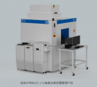
Yuwei Semiconductor's first i6R-210 mask panoramic quality management product was successfully shipped.​


Yuwei Semiconductor's first i6R-210 mask panoramic quality management product was successfully shipped and delivered to the domestic advanced mask production plant. The i6R-210 shipped this time is a mask panoramic quality management equipment that integrates defect detection, double-sided cleaning and plate inversion functions first launched by Yuwei.

The i6R-210 product, as the third generation product of the Yuwei i6R product line, has inherited the characteristics of the previous two generations of products, such as high productivity, high-precision bright and dark field detection system, and convenient operation. Through the introduction of a number of advanced technologies and function optimization, the successful Extend the application scenario from the yellow light area of the previous fab to the mask room, and to the reticle production plant. At the same time, relying on Yuwei's original 360° lighting technology, i6R-210 products have gradually begun to establish a unified closed-loop management standard system for mask factory shipment inspection and wafer factory warehouse inspection.

1691588652441.png

In the fab, the Yuwei i6R-210 product can be used in the yellow light area to control the mask quality before and after exposure. Compared with the traditional particle detection method on the surface of the reticle, the defect types that the i6R-210 product can detect are more comprehensive and reliable, so as to help customers avoid large batches of wafers being scrapped due to missed detection of some special defect pollutants. At the same time, in the photomask room, the i6R-210 product can be applied to the incoming inspection of the reticle and regular defect monitoring, which is convenient for customers to manage the reticle.

Please, Log in or Register to view URLs content!
 

tokenanalyst

Brigadier
Registered Member

Zhongke Huiyuan's first compound semiconductor (SIC) defect detection equipment was delivered smoothly.​

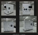
On August 5, 2023, the first compound semiconductor (SIC) defect detection equipment independently developed by Zhongke Huiyuan South China Product Center was successfully delivered to the industry's leading customer site. This marks an important step taken by the company in the semiconductor industry, further consolidating Zhongke Huiyuan's leading position in technological innovation and product quality.

1691588880417.png
Compound semiconductor (SIC) defect inspection equipment is an advanced defect inspection equipment specially developed by Zhongke Huiyuan for manufacturers of SIC (silicon carbide) wafer materials. As an emerging wide bandgap semiconductor material, SIC has excellent performance advantages in the fields of high-power electronic equipment, new energy and photovoltaics.

In order to solve this challenge, Zhongke Huiyuan has used its many years of experience and technical advantages in the defect detection industry to develop a series of silicon carbide defect detection products (CSU100, CSU200, CSU030 series) , which can be applied to silicon carbide substrates and epitaxy Product process inspection, shipment inspection and other requirements. The CSU030 device shipped this time combines advanced optical imaging technology, image processing algorithm and artificial intelligence analysis technology. Through the ultra-micro imaging system, it has bright field and dark field imaging methods and adopts sub-micron resolution, which can be efficient and accurate. It can accurately detect various defects in SIC materials, including cracks, scratches, dirt, pits, micropipes, wrapping, dislocations and stacking faults.

The semiconductor industry is known as the "crown" of the manufacturing industry, and it is also one of the most important application areas of machine vision. In recent years, in the field of semiconductor back-end packaging and testing in my country, the main equipment has been close to localization; we still face many difficulties in the front-end equipment. Taking wafer testing equipment as an example, it has been monopolized by foreign giants for a long time and has high technical barriers. It is a "stuck neck" field that my country's semiconductor industry needs to break through. Zhongke Huiyuan has always paid close attention to the semiconductor field. The company's years of technical experience and human resources in the field of industrial visual appearance inspection have provided a strong guarantee for the shipment of the first silicon carbide defect inspection equipment.

Please, Log in or Register to view URLs content!
 

tokenanalyst

Brigadier
Registered Member

The first set of shipments of semiconductor equipment on the OCTOPUS platform of PUDAT Technology has entered the fast lane​


On August 8, Prodart Technology, which is listed on the Hong Kong Stock Exchange , held the first shipment ceremony of the OCTOPUS platform in the Electronic Information Industrial Park of Xuzhou High-tech Zone.

Liu Erzhuang, CEO of Putat Technology , said that the new OCTOPUS semiconductorThe first set of single-chip cleaning equipment platform was shipped, marking that Pudae Semiconductor and Pan- Semiconductor equipment business has entered the fast lane. With the support of Xuzhou Municipal Government's industrial policy, Putat Technology will continue to invest in research and development, continue to improve equipment performance and develop new products. At the same time, the company will actively deploy new business segments, provide customers with advanced, stable and reliable core equipment, and contribute to the early realization of semiconductor equipment independence.

1691589878354.png
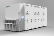
OCTOPUS products of Pudat Technology​

As an important member of the semiconductor equipment industry, Putat Technology gathers a core team with leading technical advantages and experience in the industry to carry out self-research on semiconductor equipment, aiming at semiconductor wafers and solar energyBattery The core process equipment of the manufacturing industry combines the latest semiconductor equipment technology with pan-semiconductor electromechanical automation technology to develop high-productivity equipment and actively promote the localization of the semiconductor equipment industry.

According to the 2022 financial report, Pudat Technology's semiconductor equipment and solar equipment business revenue accounted for 67% of revenue.

According to the R&D personnel of Putat Technology, in the field of semiconductor equipment, the business of Putat Technology mainly includes two platforms: CUBE series and OCTOPUS series. The semiconductor cleaning equipment shipped this time is the first product of the OCTOPUS platform. OCTOPUS series semiconductor cleaning equipment is in the leading position in the industry in terms of size, process performance, production capacity, throughput, etc., and the throughput is 17-25% higher than similar products.

According to the plan, the production capacity of semiconductor cleaning equipment at the Pudat Technology Production Base in Xuzhou is 100 units per year.
 

tphuang

Lieutenant General
Staff member
Super Moderator
VIP Professional
Registered Member
It goes both ways. Even Qualcomm sell some SoC with builtin modem. They can either include the modem as part of the SoC or supply as a separate module. As I said in my post Huawei used 5G modem as a separate module on Mate 20x 5G, because the SoC it used was Kirin 980, which already had a 4G modem baked into it. Therefore that phone technically had two modems but only the external 5G one was used.
But when they released Mate 30 they had incorporated the 5G modem directly into the Kirin 990 SoC, similar to the way they had a 4G modem in the Kirin 980. You can check the board of that phone and see there is no extra modem. Not only that they also stacked the RAM on top of the SoC. So on that phone for real estate purposes the SoC + Modem + RAM is occupying a single space.
Stacking dies does not change the situation if you are HW. You still need x amount of die surface area you need to fab per phone. That's the question all along. Given SMIC's limited capacity, how many phone's SoC and 5G modem can it fab?

Based on all the ongoing rumors, HW's 5g modem is using 12/14nm process whereas SoC is using 7nm process. Without access to N5 process, Hisilicon has to get creative.
Here also I was specifically talking about Mate 30. In that they did not use American RF. My point was to say that it was doable without American RF even 4 years ago. And I think Huawei's point was also to demonstrate that it is doable, because they re-introduced American parts in Mate 30 pro.
Here is a comparison of parts suppliers for Mate 30 vs phones before that. And as I said they started using American parts again on subsequent phones. At the time Huawei didn't know the extent of US sanctions going to be so they made Mate 30 without US parts, to demonstrate their ability to do so. But they kept using other chips in subsequent models because they were still allowed to buy those or had stock.
View attachment 116987
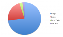
If you take a look at the BAW filter market share, you'd see that American companies control 95% market share. Where is Murata? I don't see them. Yes this UBS report thinks Murata is supplying them the RF filters
22165971_14570185873015_1.png
So I'm entirely unconvinced with the findings that Mate 30 was actually devoid of American components.

Let's say they are one of 2% of phones that use Taiyo Yuden BAW filters. Would it actually have satisfactory performance for a flagship phone? If not, then what's the point? After all, there have also been BAW filters from Chinese producers for a few years (huntersun), but it doesn't look like any prominent phone maker used them in a 5G phone. The recent news of Silex & Memsonics is only relevant because Memsonics claims to have achieved leading performance with them.

And more importantly, the goal of Huawei needs to be 100% domestic. Using Japanese & Dutch RF components don't mean anything as we've seen.
 

tokenanalyst

Brigadier
Registered Member

Fuxuan Technology received a new round of financing for the construction of the Hefei headquarters production base​


According to news from Weiwang, recently, Yida Capital completed the investment in Shanghai Fuxuan Automation Technology Co., Ltd. (referred to as: Fuxuan Technology). This round of financing will be used for the continuous R&D investment of Fuxuan Technology and the construction of the production base of the Hefei headquarters.

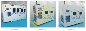
Founded in 2016, Fuxuan Technology is a professional chemical delivery system (CDS), raw liquid delivery system (SDS), recycling mixing system (SRS), and electronic grade chemical mixing in the semiconductor, high-purity chemical, and photovoltaic industries. , purification, filling, conveying system (Chemicals System) and wet cleaning equipment (Wet Bench) and other scientific and technological enterprises integrating R&D, production, sales and service. It is committed to providing wet chemical customers with high-purity chemical purification, Packaging and delivery system solutions.

According to information from Yida Capital, the application of Fuxuan Technology products covers semiconductors, solar energy, liquid crystal panels, optical fibers, high-purity chemicals and other production fields. Long-term domestic and foreign customers of Fuxuan Technology include Changxin Storage, LONGi Green Energy, Anji Technology, Zhongxin Wafer, Shanghai Xinyang, China Resources Microelectronics, Tianma, Japan SDP Super Vision Display and other enterprises.​

1691591545021.png

Please, Log in or Register to view URLs content!
 

tokenanalyst

Brigadier
Registered Member

Huada Jiutian (Empyrean EDA) fully develops the automotive electronics market——the product has obtained ISO 26262 TCL3 and IEC 61508 T2 international standard certification​


On August 3, 2023, Empyrean Polas ®, the reliability analysis tool of Huada Jiutian, obtained the ISO 26262 TCL3 and IEC 61508 T2 international standard certification. At the same time, various digital and analog EDA products of Huada Jiutian will pass the ISO 26262 TCL3 and IEC 61508 T2 product certifications within this year.

With the rapid development of the global automotive electronics industry, electrification, intelligence, and networking are the three most important trends, and they all require the strong support of automotive-grade chips and EDA tools. Over the years, Huada Jiutian has been working hard in the field of industrial control and automotive electronics, and has created a relatively complete domestic EDA solution for automotive electronics, including automotive analog EDA tools, automotive digital EDA tools, and automotive flat panel display EDA tools. plan. This time, Empyrean Polas ® was the first to obtain the certification of ISO 26262 TCL3 and IEC 61508 T2 international standards, which not only reflects the strong technical strength of Huada Jiutian in the EDA field for many years, but also demonstrates that the company takes products as the core and application solutions as the traction industry leadership. As a leading domestic EDA company, Huada Jiutian is actively participating in the construction of domestic independent automotive electronics EDA standards while obtaining international standard certification.

Empyrean Polas ® is a reliability analysis tool focused on the design of power management chips provided by Huada Jiutian to solve the design dilemma of power management chips. Empyrean Polas ® provides a system analysis solution by integrating a variety of tools from Huada Jiutian, and provides designers with a comprehensive picture of power management chips in terms of distributed, highly reliable on-resistance, electromigration and voltage drop, and gate delay analysis. Analysis, its one-stop complete solution provides a guarantee for designers to sign off on power management chips and improve their yield. At present, it has been purchased by many domestic and foreign automotive-level power management chip design companies, and is widely used in the design process of automotive discrete MOS devices, SiC devices and high-power control chips.

Please, Log in or Register to view URLs content!
 
Status
Not open for further replies.
Top