Chinese semiconductor industry

Status
Not open for further replies.

tokenanalyst

Brigadier
Registered Member

Gaoce's revenue in the first half of the year exceeded 2.5 billion yuan, and silicon carbide slicers have formed batch orders​


, Gaoce released the 2023 semi-annual report, the company achieved operating income of 2.521 billion yuan, a year-on-year increase of 88.80%; achieved net profit attributable to shareholders of the parent company of 714 million yuan, a year-on-year increase of 201.27% ; Realized a net profit of 692 million yuan after deducting non-existing expenses, a year-on-year increase of 197.40%.

Gaoce shares said that during the reporting period, the photovoltaic industry continued to maintain a high booming development trend, and the demand for photovoltaic cutting equipment was strong. The GC700X slicing machine, GC-700XL slicing machine, GC-800XP slicing machine, GC-MK202R double ring wire squaring machine, GC-MK202RG grinding and grinding machine and GC-GP950L grinding and polishing machine and other photovoltaic equipment launched by the company are famous for their sustainable development. The leading technical advantages are continuously recognized by customers, the leading effect is remarkable, and multiple products work together, ranking first in market share. During the reporting period, equipment orders increased significantly and a relatively stable gross profit margin was maintained.

During the reporting period, the company's photovoltaic cutting equipment products achieved a total operating income of 808.1267 million yuan, a year-on-year increase of 44.23%. As of June 30, 2023, the total amount of orders in hand for the company's photovoltaic cutting equipment products was 2.77 billion yuan (tax included), a year-on-year increase of 135.54%.

In the field of photovoltaic cutting consumables, during the reporting period, relying on the advantages of closed-loop technology research and development, the company continued to lead the industry to promote the iteration of diamond wire thinning. The company has achieved batch sales of 36μm, 34μm and below diamond wires, and has led the industry in launching 30μm wires Diamond wire, the company is actively carrying out research and development and testing of thinner high-carbon steel wire diamond wire and tungsten wire diamond wire to promote the continuous progress of the industry's cutting technology. During the reporting period, the company's photovoltaic cutting consumables realized revenue of 690.1558 million yuan, a year-on-year increase of 111.69%.

1691424312513.png
Please, Log in or Register to view URLs content!
 

tokenanalyst

Brigadier
Registered Member

Huafeng Technology received tens of millions of dollars in strategic financing​


According to 36 Krypton reports, recently, Huafeng Technology has completed tens of millions of dollars in strategic financing, led by Zhilu Capital. This round of financing will be mainly used for production research and development and market expansion.
Founded in 2014, Huafeng Technology is a high-end equipment manufacturer focusing on the field of advanced packaging equipment, and is committed to providing product technologies and solutions for advanced semiconductor packaging. The company's products have achieved comprehensive coverage of advanced packaging and placement processes, including FOWLP (Face Up/Down), POP, MCM, EMCP, Stack Die, SIP, 2.5D/3D, FCCSP, FCBGA, etc.
Huafeng Technology is positioned in the field of advanced semiconductor packaging, and provides a new generation of semiconductor assembly and packaging equipment for semiconductor back-end processes, such as flip-chip placement machines, wafer-level placement machines, POP packaging machines, stacked half placement machines, panel Level placement machine, multi-chip placement machine, etc.
It is reported that the clients that Huafeng Technology serves include ASE, Siliconware, Changdian Technology, Huatian Technology, Tongfu Microelectronics, etc.

Please, Log in or Register to view URLs content!
 

tokenanalyst

Brigadier
Registered Member

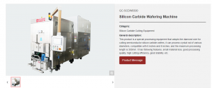
Silicon carbide material production project signed in Huai'an, Jiangsu​

The silicon carbide material production project was introduced by the Organization Department of the District Committee, and invested and constructed by Hong Kong Keting Intelligent Co., Ltd. The project is located in the north of Guangzhou Road and east of Jingjiu Road, covering an area of about 70 acres, with a construction area of about 60,000 square meters. The new production line for the preparation, sintering, processing, purification and cleaning of semiconductor silicon carbide powder and products.

The chairman of Hong Kong Keting Intelligent Co., Ltd. said that Keting Intelligent is a high-tech company facing the world's technological frontiers, the main economic battlefield, and the country's major needs. This signing is an in-depth cooperation with the Huaian District Government on the silicon carbide project, and is committed to promoting the high-quality development of the semiconductor industry.
 

tokenanalyst

Brigadier
Registered Member

Startup Funding: July 2023​


EDA​

GWX Technology raised
Please, Log in or Register to view URLs content!
(CNY 100.0M is ~$13.9M) in financing led by Essence Capital and Guangzhou Lifeng. GWX Technology develops back-end design and verification tools, including SPICE simulation, characterization, formal equivalence checking, design for test, physical verification, optical proximity correction, and yield analysis. The company also offers IP, SoC, DFT, and package design services. Founded in 2018, it is based in Shenzhen, China.

Manufacturing & equipment​


Demark Precision Technology received CNY 100.0M (~$13.9M) in Series A financing from Great Stone Capital, Addor Capital, and others. The company offers
Please, Log in or Register to view URLs content!
of parts for semiconductor manufacturing equipment, wind turbines, and robotics. Founded in 2016, it is based in Huzhou, China.

XIVI Technology raised nearly CNY 100.0M (~$13.9M) in a Series A round led by Glory Ventures, joined by Ivy Capital and others. XIVI offers
Please, Log in or Register to view URLs content!
, wafer stages, and wafer transfer systems. Funds will be used for R&D and to expand operations and production. Founded in 2015, it is based in Wuxi, China.

Using.AI drew tens of millions of yuan (CNY 10.0M is ~$1.4M) in pre-Series A financing from Legend Capital and GSR United Capital. The startup develops AI solutions for
Please, Log in or Register to view URLs content!
in advanced manufacturing, including displays, optics components, and semiconductors. Founded in 2017, it is based in Shenzhen, China.

Aerotech drew new financing from China Electronics Research and Investment Fund, Changsha Pilot Investment Holdings, and others. The company makes gas pipe
Please, Log in or Register to view URLs content!
for semiconductor manufacturing equipment. Founded in 2008, it is based in Beijing, China.

Joysingtech Semiconductor drew investment that included automaker BYD. Joysingtech makes semiconductor manufacturing equipment, including for etch, thin film deposition, and rapid thermal annealing. Founded in 2021, it is based in Jiaxing, China.

Packaging​

Jiangsu IC Assembly & Test (ICAT) raised hundreds of millions of yuan (CNY 100.0M is ~$13.9M) in financing led by Jintong Capital. ICAT provides
Please, Log in or Register to view URLs content!
. Its capabilities include wirebond packages (SOP/SOT, QFN/DFN, QFP, LGA) as well as flip-chip system-in-package and wafer-level chip-scale packages. Funds will be used to expand production capacity and for R&D. Founded in 2018, it is based in Xuzhou, China.

Test, measurement & inspection​

Zenfocus Semiconductor Technology raised
Please, Log in or Register to view URLs content!
(CNY 100.0M is ~$13.9M) in a Series C round. Zenfocus provides
Please, Log in or Register to view URLs content!
for wafers and finished products, including ATE test boards, high-speed 2D/3D MEMS probe cards, multi-layer organic substrates, multi-layer ceramic substrates, and memory probe cards. Funds will be used for capacity expansion, equipment procurement, R&D, and market development. Based in Shanghai, China, it was founded in 2015.

Zhongan Semiconductor raised hundreds of millions of yuan (CNY 100.0M is ~$13.9M) in Series A+ funding from Fengyuan Capital, CoStone Capital, China Fortune-Tech Capital, Oriza Holdings, and others. The company makes wafer inspection and metrology equipment, including non-contact optical interferometry for parameters such as wafer warpage, flatness, thickness, and film stress. It also offers particle defect detection equipment. Founded in 2020, it is based in Nanjing, China.

Avant Semiconductor raised
Please, Log in or Register to view URLs content!
led by Cornerstone Pujiang, followed by New Hope Capital, Galaxy Capital, South China Venture Capital, Honghu Capital, and others. Avant Semi provides front-end inspection and measurement equipment. Its products include an automated epitaxial film thickness and element measurement system that uses Fourier-transform infrared spectroscopy (FTIR) for non-destructive, high-sensitivity analysis. Along with epitaxial layers, it can also measure photoresist thickness, CMP polished thickness, and element concentrations. It also offers optical defect detection equipment for silicon carbide wafers. Founded in 2021, it is based in Shanghai, China.

Optics Robot Technology raised nearly CNY 100.0M (~$13.9M) in Series B funding from CICC Capital and others. The company offers
Please, Log in or Register to view URLs content!
(AOI) and laser marking equipment for semiconductor packaging, PCBs, and displays. Founded in 2016, it is based in Nanjing, China.

LightE Technology received
Please, Log in or Register to view URLs content!
(CNY 10.0M is ~$1.4M) in strategic financing from Keli Sensing Technology. LightE Technology makes spectral confocal displacement sensors for 3D optical inspection of semiconductors, PCBs, consumer electronics, photovoltaics, lenses, and other applications. The startup says the technology has higher precision, wider material adaptability, and higher stability compared to traditional lasers. It currently offers point and linear confocal sensor products. Based in Shenzhen, China, it was founded in 2014.

DKW Micro received nearly CNY 10.0M (~$1.4M) in angel funding from Weixi Capital. The company makes ATE and PCB test probes. Founded in 2010, it is based in Suzhou, China.

DeepSight Information Technology drew
Please, Log in or Register to view URLs content!
from SND Financial Holdings and CEC Fund. DeepSight provides an automated visual inspection platform for wafers, PCBs, flexible PCBs, and high-density interconnector PCBs. It uses computer vision and reinforcement learning techniques to detect defects. Founded in 2017, it is based in Shanghai, China.

Materials​


Gao Semi raised CNY 65.0M (~$9.1M) in Series A funding from V Stone Fund, Haitong Securities, and others. The startup manufactures gallium oxide single crystal and epitaxial wafers. Funds will be used for R&D, capacity expansion, and hiring. Founded in 2021, it is based in Beijing, China.

Tanrand Technology drew tens of millions of yuan (CNY 10.0M is ~$1.4M) in angel financing from CasStar and Trustino Capital. The company manufactures
Please, Log in or Register to view URLs content!
, films, and aerogels and graphene/copper composite powders for applications including conductive pastes and electromagnetic shielding. The company also makes stir friction welding equipment. Founded in 2015, it is based in Beijing, China.

Bolai Narun Electronic Material, also known as Planary, received new investment from Su Venture Capital and SIDVC. The company makes abrasive particles, polishing liquid, and polishing pads for chemical mechanical polishing (CMP) in manufacturing semiconductor wafers, LED sapphire substrates, and optical glass. Founded in 2021, it is based in Suzhou, China.

BYN Chemical received
Please, Log in or Register to view URLs content!
led by CD Capital, Fortune Capital, and GAC Capital. The company manufactures various
Please, Log in or Register to view URLs content!
, including the solvent NMP, for the electronics, LED, battery, and other manufacturing industries. Founded in 2011, it is based in Binzhou, China.

TC Ceramic Electronics drew
Please, Log in or Register to view URLs content!
from SDIC Venture Capital. The company makes
Please, Log in or Register to view URLs content!
for power electronics. It offers both direct bonded copper and active metal brazed ceramic copper clad laminates, including DBC zirconium-doped Al2O3, AMB-Si3N4, and AMB-AlN. Founded in 2013, it is based in Jiaxing, China.

Wylton Jinglin Electronic Material raised pre-IPO financing led by Lanhor Capital. The company provides a range of
Please, Log in or Register to view URLs content!
including POCl3, BBr3, TEOS, TMA, and DCE for IC, discrete, photovoltaic, and LED thin film deposition and manufacturing. Founded in 2006, it is based in Guiyang, China.

Please, Log in or Register to view URLs content!
 

caudaceus

Senior Member
Registered Member
Using.AI drew tens of millions of yuan (CNY 10.0M is ~$1.4M) in pre-Series A financing from Legend Capital and GSR United Capital. The startup develops AI solutions for
Please, Log in or Register to view URLs content!
in advanced manufacturing, including displays, optics components, and semiconductors. Founded in 2017, it is based in Shenzhen, China.
Lmaoo this so cheat.
There will be having.ai doing.ai making.ai growing.ai taming.ai etc next.
 

horse

Colonel
Registered Member

Tech war: China's memory chip efforts face stronger headwinds as Micron, Samsung, SK Hynix race ahead on AI​

Please, Log in or Register to view URLs content!

This story is very bizarre.

Suppose we want to buy a desktop.

We would compare features, the specs, and the prices, and we decide what to buy. That is very basic. We look at what is being offered for sale by different vendors and we choose.

But the article does not do that. It should have at least listed the main sellers of memory chips and told us what they sold, their best products, solid state drives, so on and so forth.

No reason to bring up the AI angle. Did they know the difference between a logic chip, a microprocessor, and random access memory?

That is why this is so weird this article.

They got someone to write an article about memory chips who never bought a computer before in their life.

That the article is rubber stamped by an editor and published, then picked by Yahoo.com and republished, is kind of remarkable.

:D
 

tokenanalyst

Brigadier
Registered Member
Interesting read

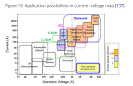
Past, present, and the future of the research and commercialization of CVD diamond in China​

Abstract​

It has been half of a century since the publication of the early reports about CVD diamond films in the world in the early 1970’s. The reports for meaningful laboratory growth of diamond films with much higher growth rate and higher quality could be found in the early 1980’s, under the so-called “Diamond Fever” initiated all over the world. In less than 10 years later, CVD diamond research had started in China as “863 Plan” (High Technology Research and Development Plan in China), a newly launched program in 1987. 35 years later, it is very interesting to explore what really happened to the CVD diamond in China. As a multi-functional material with a vast combination of extraordinary electrical, mechanical, thermal, optical, acoustic, and electro-chemistry properties, the CVD diamond has wide applications potentially in the field of multidiscipline high technologies. Therefore, this article aims to provide a general review on the CVD diamond by presenting a clearer picture about the history, the research status and its development, particularly the commercialization in China. Finally, the general trend in the near future is discussed.

1691442732457.png

Please, Log in or Register to view URLs content!
 

FairAndUnbiased

Brigadier
Registered Member
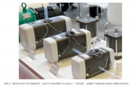
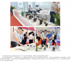
Maglev pumps for Ultrapure Water transport, necessary for immersion lithography and other semi manufacturing areas.
View attachment 116917View attachment 116919

Please, Log in or Register to view URLs content!
I wouldn't say it's totally maglev, only magnetically coupled. You can actually buy stainless magnetically coupled water pumps on AliExpress for $200 USD which are clean enough for pharmaceutical grade manufacturing (only wetted components are PEEK and 316 stainless). For even higher purity you'd just coat stainless with PVDF.

Please, Log in or Register to view URLs content!
 
Status
Not open for further replies.
Top