
You are using an out of date browser. It may not display this or other websites correctly.
You should upgrade or use an alternative browser.
You should upgrade or use an alternative browser.
Chinese semiconductor industry
- Thread starter Hendrik_2000
- Start date
- Status
- Not open for further replies.
SIOM is researching EUV masks, EUV metrology, materials and computational lithography. CIOMP is researching the mirrors and optical sub-systems. Hangzhou the high power lasers, there a like three efforts in making the droplet generators and so on.Based on the progress of all the patents (especially light source), i'm under the impression that both SIOM & CIOMP are working on their own EUV prototypes and CAS is pretty involved in all of this. Timeline wise, if they can get an alpha prototype assembled this year, it would be quite the miracle. At this point, I see EUV project about 3 years behind SSA800 for entering high volume production, which would shock pretty much everyone. I don't know how everyone else looks at it.
If you look at the TrumpF CO2 MOPA light source, the machine is an absolute monster when it comes to how complex it is. Their website lists their drive laser as having more than 457000 parts, 7km of cabling, weighing 17 tonnes with the entire setup requiring more than 30 metres of space. It really isn't any wonder why the thing was so difficult to develop and manufacture. A much simpler drive laser (like the fibre laser previously discussed in the thread) would cut down considerably on cost and complexity.If I remember correctly, ASML struggled with the light source in order to build a productive EUV system? The other components of the machines are easier?
Is there any information regarding the app that is developed by ChunhChun institute of Optics use? Also MPOA laser?If you look at the TrumpF CO2 MOPA light source, the machine is an absolute monster when it comes to how complex it is. Their website lists their drive laser as having more than 457000 parts, 7km of cabling, weighing 17 tonnes with the entire setup requiring more than 30 metres of space. It really isn't any wonder why the thing was so difficult to develop and manufacture. A much simpler drive laser (like the fibre laser previously discussed in the thread) would cut down considerably on cost and complexity.
There's information posted in this thread about the development of MOPA lasers and optics.Is there any information regarding the app that is developed by ChunhChun institute of Optics use? Also MPOA laser?
Last edited:
Guangzhou Xingsen will receive a capital increase of 1.605 billion yuan to promote the construction of FCBGA packaging substrate projects
Shenzhen Xingsen Express Circuit Technology Co., Ltd. ("Xingsen Technology") held the twenty-fourth meeting of the sixth board of directors on August 2, 2023, and reviewed and approved the "Regarding the Capital Increase of Subsidiaries and the Introduction of Strategic Investors" "Proposal", agreeing to increase the capital of Guangzhou Xingsen Semiconductor Co., Ltd. ("Guangzhou Xingsen") and introduce strategic investors

Guangzhou Xingsen is a holding subsidiary of Xingsen Technology. In order to promote the construction process of the FCBGA packaging substrate project, it plans to increase the capital of Guangzhou Xingsen and introduce 5 strategic investors. shares, all included in the registered capital, of which, Xingsen Technology plans to subscribe for a capital contribution of 555 million yuan, CDB Manufacturing Transformation and Upgrading Fund (Limited Partnership) plans to subscribe for a capital contribution of 450 million yuan, CCB Financial Assets Investment Co., Ltd. plans to subscribe for a capital contribution of 450 million yuan Subscribed capital of 250 million yuan, Henan Asset Jianyuan Stable Development Equity Investment Partnership (Limited Partnership) intends to subscribe for a capital contribution of 100 million yuan, Jiaxing Juli Zhanye No. 10 Equity Investment Partnership (Limited Partnership) intends to subscribe for a capital contribution of 20,000 RMB 10,000, and Guangdong Yueke Venture Capital Co., Ltd. intends to contribute RMB 50 million. The amount of capital increase by all parties shall be subject to the final paid-in amount. All parties to this capital increase will contribute capital in the form of currency, and the sources of funds are all self-raised funds of each party. The time for payment of the capital increase is subject to the agreement in the investment agreement.
After the completion of this capital increase, the registered capital of Guangzhou Xingsen increased from 600 million yuan to 2,205 million yuan. Xingsen Technology directly holds 47.85% of Guangzhou Xingsen's equity, and indirectly through Zhuhai Juli, Zhuhai Juxian and Zhuhai Juzhi. Guangzhou Xingsen 4.53% stake, Guangzhou Xingsen is still a subsidiary of Xingsen Technology Holdings.
On separate topic, from Infineon earnings call
Looks like SICC & TanKeBlue already up to 20% of substrate for Infineon and probably will get to 40 to 50% depending on how much of the demand is from China. This imo still does not change the fact that Infineon is not invested into China like ST (which is both sourcing sic wafers & producing sic modules in China with Sanan)
But it is good to know that SICC and TankeBlue are qualified for auto chips. more chinese sic players should use them
Yeah, and I take the silicon carbide part. So we're very happy with the progress we make with these two Chinese silicon carbide supplier SICC and TanKeBlue. We announced last quarter, as I stated, they are automotive qualified now. [To us], they contribute already 20% to the volume as we speak, last quarter and this share will likely double and then go in line with the local demand in China. With respect to their own yields, you need to -- our yield is absolutely on a very good level also compared to other suppliers. Their own yields, I can only speculate but I can assure you, the material we get whether its boules or wafers are of very high quality.
Looks like SICC & TanKeBlue already up to 20% of substrate for Infineon and probably will get to 40 to 50% depending on how much of the demand is from China. This imo still does not change the fact that Infineon is not invested into China like ST (which is both sourcing sic wafers & producing sic modules in China with Sanan)
But it is good to know that SICC and TankeBlue are qualified for auto chips. more chinese sic players should use them
he works at Changchun Research Institute... and LPP-EUV will be tested from Q1 next yearThank you @pbd456 , @measuredingabens bro regarding your inquiry and our discussion hope this help.You may connect the dots and come to your conclusion.

Regarding the semi-official news from Huawei insiders, could it be that the trial operation of the EUV machine was successful?
71 people liked this article
A netizen named "erichain" on Weibo turned out to be the focus of Huawei executive Yu Chengdong. Netizens familiar with the situation claimed that he was an internal employee of Huawei. Huawei has more than 200,000 employees. It can be seen that an employee can get the attention of Huawei executives. This person is not simple, and there is a high probability that he is Huawei's "technical master".
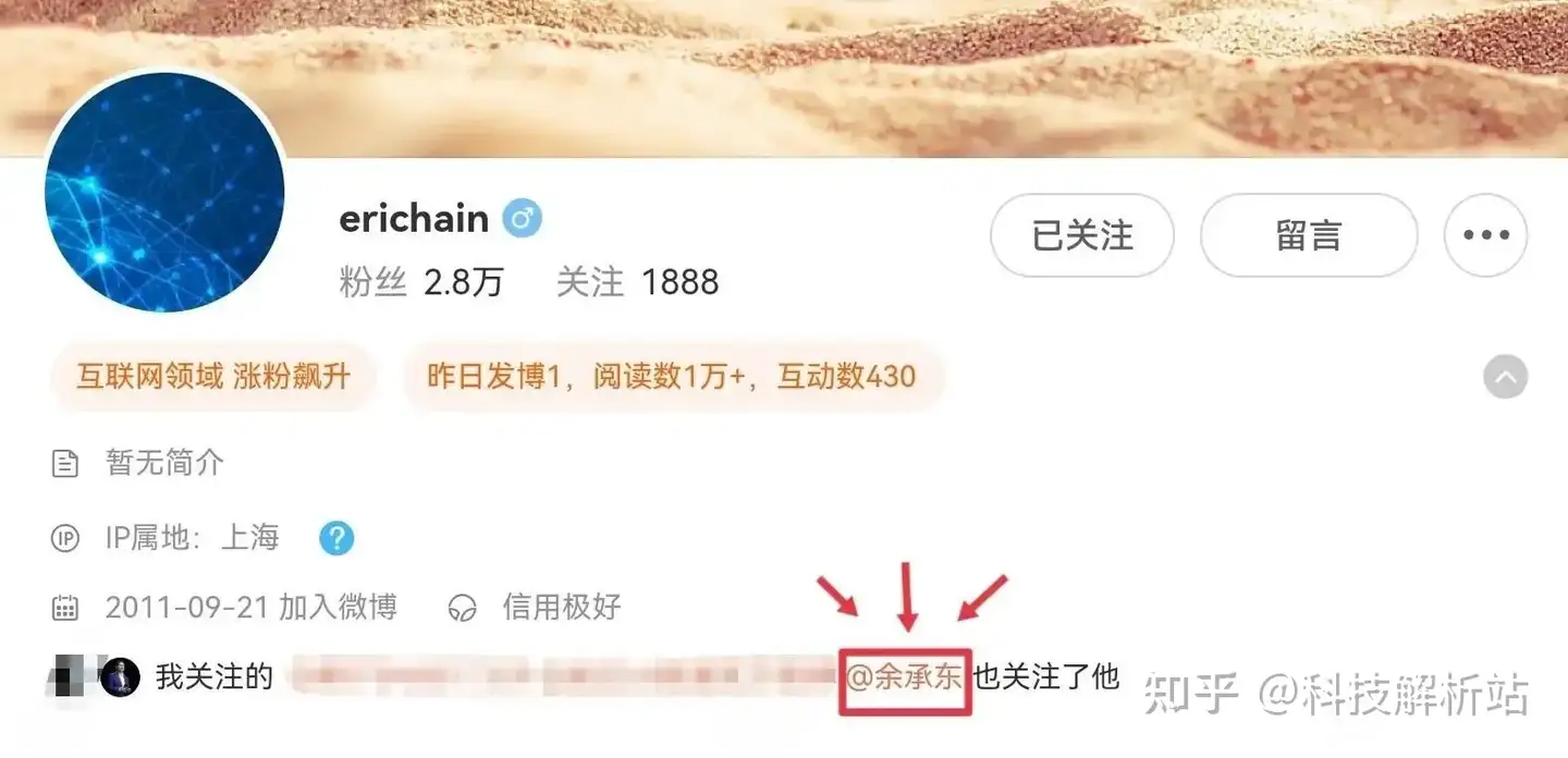
At the beginning of 2021, there were gossip that Huawei had dispatched elite troops to help domestic scientific research units accelerate their research and development progress, but it was a pity that it was not confirmed by any official organization.
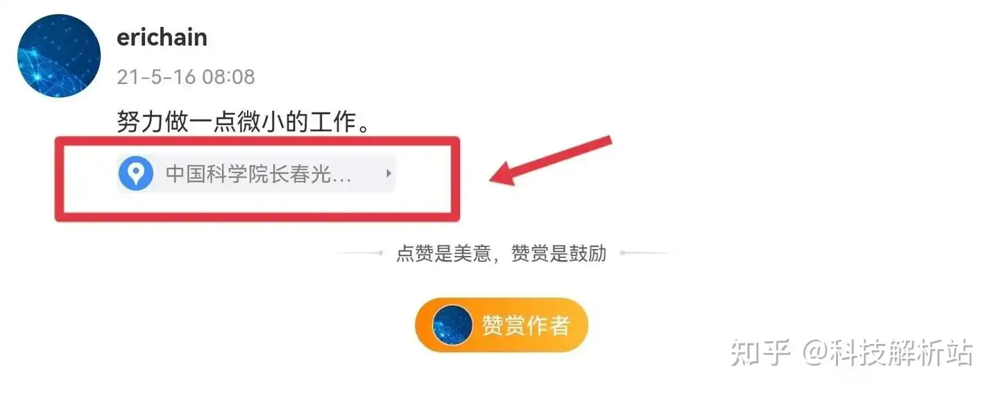
On May 16, 2021, "erichain" posted a Weibo post "try to do a little work", and the location of the post was shown at the Changchun Institute of Optics and Mechanics, Chinese Academy of Sciences. This place is amazing! It is the research and development base of my country's LPP-EUV light source. Some netizens speculated that in May 2021, the appearance of "erichain" in this place is likely to help this scientific research unit accelerate the development of EUV light sources.
In the first half of this year, the official website of the Changchun Institute of Optics and Mechanics published a report, introducing the good news that Academician Bai Chunli, the president of the Chinese Academy of Sciences, visited the Changchun Institute of Optics and Mechanics. According to the past practice of my country's official institutions, this means that my country has made a major technological breakthrough in LPP-EUV light source technology! Is there any help from Huawei's "technical giant"? you guess?
The EUV light source is known as the "core of the core" in the EUV front-end exposure equipment, and its successful development means that the EUV complete machine is not far away!
On July 2, "erichain" posted another Weibo saying, "Thanks to all those who have contributed to the country, to all those who have helped Huawei, and to the vast number of consumers. This year, there are some achievements in some fields, dedicated to all who have the same heart. Glory to you!"
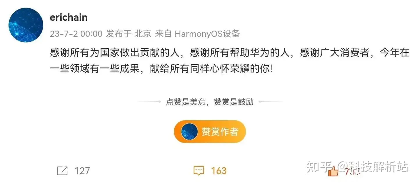
From this sentence, we can see that "erichain" was very excited at that time, and the things that made him so excited must not be trivial!
It can be seen that Huawei must have made a major technological breakthrough, and it is a major technology that can affect the development of the country! We don't know exactly what it is! Could it be that after the integration of EUV front-end exposure equipment, the trial operation was successful?
According to the official information, the EUV principle prototype independently developed by my country passed the acceptance test in 2017! On April 13, the Changchun Institute of Optics and Mechanics disclosed the news that Academician Bai Chunli, President of the Chinese Academy of Sciences, investigated the EUV light source, indicating that the EUV engineering prototype or the light source of the prototype machine has also been completed! The "erichain" message was sent on July 2, most likely because the trial operation of the EUV machine was successful! As early as 2021, some netizens revealed that domestic EUV is expected to be produced in 2023! To make this great god so excited and make such remarks can only be a major achievement for the whole machine, not a single technological breakthrough! Comprehensive judgment, the biggest possibility is that the EUV test run was successful!
I posted on twitter that Huawei is testing the light source... a few days ago
Microconductor Nano (LEADMICRO): There are equipment orders in logic chips/storage chips/compound semiconductors and other fields
On August 3, Microconductor Nano disclosed the latest survey summary, stating that the application scenarios of the company's semiconductor ALD equipment represent the development direction of process diversification in various subdivisions of domestic semiconductors. In the fields of logic chips, memory chips, new display chips, and compound semiconductors All have equipment orders, and gradually promote verification or acceptance at the client side.
The iTronix® series of CVD equipment launched by the company based on the strategic needs of customers' key process development is a new product series independently developed by Microconductor Nano based on the strategic needs of customers' key process development; it is suitable for silicon oxide, silicon nitride, silicon oxynitride, The deposition process of various thin films such as amorphous silicon can be widely used in chip manufacturing in the fields of logic, storage, advanced packaging, display devices, and compound semiconductors.
In the field of semiconductors, Microconductor Nano is the first domestic equipment manufacturer to successfully apply mass-production High-k atomic layer deposition (ALD) equipment to the front-end production line of 28nm node integrated circuit manufacturing. It has established partnerships with many domestic manufacturers In-depth cooperative relationship, related products cover logic, storage, compound semiconductor, new display and many other subdivided application fields, and many key indicators of equipment have reached the advanced level.
Microguide Nano said that as a domestic supplier of thin film deposition equipment, the company can respond quickly to customers' process and film performance needs according to the actual needs of downstream companies, and meet customer production line needs in a timely manner. The company has a sound technical service system, providing customers with timely on-site technical service support, arriving at the site in time to troubleshoot and solve problems, ensuring rapid response to customer needs, and shortening the process run-in time for new product introduction.
In terms of orders, Weidao Nano said that the company currently has ample orders in hand. In order to meet the rapidly growing order delivery needs, the company has optimized and improved the supply chain, manufacturing, and internal management to ensure on-time delivery of products and shorten the delivery period. , guaranteed delivery.
It pointed out that with the continuous evolution of Moore's Law, the feature size of integrated circuits and etched grooves continue to shrink, the complexity and process volume of wafer manufacturing have increased significantly, and advanced vacuum thin film technologies such as ALD have played an increasingly important role in the localization of semiconductor equipment. increasingly important role. Factors such as growth in demand for terminal applications, import substitution, and self-control have driven countercyclical expansion and iterative process upgrades in domestic fabs, accelerating the industrialization verification of domestic ALD equipment by top customers in the domestic semiconductor industry.
As a leading supplier of semiconductor thin film deposition equipment in China, Microconductor Nano will continue to accelerate product development, industrial verification and application in various subdivisions in the semiconductor field, and achieve breakthroughs in the localization and industrialization of a number of thin film deposition and processing technologies. While maintaining the market competitiveness and market share of ALD products, we will continue to introduce more competitive thin film deposition products such as CVD.
That's not how lithography works at all. Just because EUV is more advanced, that doesn't mean you don't need DUVi machines in other parts of the production line. Having a 22nm DUVi is still incredibly important for efficiency and cost savings. It's not like a cellphone, the newer one doesn't just automatically replace the older stuff.With the news coming from @pbd456, I'm afraid that the mythical 22nm SSA900 DUVi will never materialized.
Unless you mean over shadowed as in news and excitement, then possibly. But having a prototype also doesn't mean it's far along. It may still take a few years to go from prototype to mass production as we saw with the 28nm DUV from SMEE. It's entirely possible that the 22nm will be able to go into mass production before the EUV as well.
- Status
- Not open for further replies.