Chinese semiconductor industry

Status
Not open for further replies.

tphuang

Lieutenant General
Staff member
Super Moderator
VIP Professional
Registered Member
I think it's fair to cheer HW on and also admit that they are overly aggressive in some cases. There is a reason not everyone is using their Ascend AI chips. I would say what they are doing in auto industry is a prime example of too much

Anyhow, more of RFFE

Please, Log in or Register to view URLs content!
Anyways, Memsonics & Silex had their mass production launch ceremony on July 31st.
Memsonics CPO details the development plan for next stage of join production line. About how they can keep expanding capacity & develop tech

CTO announce a variety of new BAW filter products for Wifi, 4G & 5G. It will continue to develop new products for 5G & 6G & for next gen high frequency & large bandwidth filter products

Looks like they also had a major order signing between the 2 parties, presumably for guaranteed order

Looks like this Silex Fab 3 has been planned for a while
Please, Log in or Register to view URLs content!
it was supposed to achieve 10k wpm by end of last yr (pretty sure if hit that) and the goal is to reach 30k wpm (so 10 in phase 1 & 20k in phase 2). Phase 2 is the one with BAW filters
Please, Log in or Register to view URLs content!
according to this, Silex & Memsonics agreed to a contract back in August 2021 for the production of 8-inch wafer rf filter chips. Out of the 81 equipment, Silex paid for 35 & memsonics paid for 46. Over time, Memsonics expected to order at least 9k wpm of the MEMS product after Silex reaches 10k wpm in capacity
so the two parties really worked hard together to achieve this

Please, Log in or Register to view URLs content!
From this
武汉敏声订单9000片/月,门槛极高的MEMS BAW滤波器独家供应华为5G;

珠海开元订单10000片/月,门槛极高的MEMS BAW滤波器产品供应全球前10家BAW滤波器/模组中的6家。
out of the 20k wpm expected production, memsonics signing for at least 9k wpm eventually in order to be the sole suppliers of BAW for Huawei. Looks like Huawei has given at least 2 tech development contract to memsonics in the past for RF development. knowing HW, they probably have people working at Memsonics right now.
Looks like this zhuhai kaiyuan company will also order 10k wpm with the goal of supplying 6 out of top 10 BAW filter/modules companies

goal is to produce all the Wifi/5G/6G BAW filter chips locally.
 

taxiya

Brigadier
Registered Member
Wow sounds like Huawei is behaving almost like Tencent. Or Microsoft or Google or Amazon. Wait, or just about any tech company that succeeded anywhere. Maybe Huawei should stop being mean and aggressive by learning from the great companies that ended up being absorbed by or forced out of business by bigger more aggressive companies instead.
Depends on perspective. All those companies that you talked about are private companies in capitalist states whose only rule is the jungle rule, one kills everyone else.

China is not capitalist state, a private company's success means NOTHING to the general public if not serving the good for the whole population. The only judgement of any company's value is if it promote the industrial and technical compability of the WHOLE country. One super powerful company in a monopoly position is certainly against that purpose.

Example, there were two railway companies (south and north) in China. They competed one another in lowering prices abroad. They are essentially bleeding China's treasure by firecefully beating each other. Their own good is bad for the country. Therefor we saw them being merged into one recently. They are all state companies, so it is easier to handle. I am not advocating same dealing of Huawei, far from it. But certain limit must be set so it is not Chinese company killing another Chinese company.

Huawei is NOT a national hero, it is a commercial company whose primary aim is its own profit, which is not always in line with the national interest.
 

sunnymaxi

Captain
Registered Member
Example, there were two railway companies (south and north). They compete one another in lowering prices abroad. They are essentially bleeding China's treasure by firecefully beating each other. Their own good is bad for the country. Therefor we saw them being merged into one recently. They are all state companies, so it is easier to handle. I am not advocating same dealing of Huawei, far from it. But certain limit must be set so it is not Chinese company killing another Chinese company.
sir it was an old news. Huawei poached 150+ engineers from SMEE in 2021. everything has been sorted out and now they all are working together.

SMEE growing exponentially. from few hundred people to 2000+ in Research and development in just few years.
 

tokenanalyst

Brigadier
Registered Member
Naura updated their Chinese website adding their new solutions for bevel, compound semiconductor, TSV and their new deposition tools.
This company is a semiconductor powerhouse.

Plasma etching equipment​

Plasma dry etching technology is a technology that uses plasma for thin film microfabrication. Due to its good anisotropy and process controllability, it has been widely used in the field of semiconductor basic product manufacturing.

Relying on the accumulation and innovation in plasma control, reaction chamber design, etching process technology, and software technology, NAURA can provide Advanced equipment and process solutions. North Huachuang has now formed a full coverage of the etching process, and has the ability to etch various materials such as silicon, deep silicon, metal, dielectric, compound semiconductor (SiC, GaN, GaAs, InP, LiNb O₃ , LiTa O₃ , etc. ) Ability, with excellent process performance to become the customer's first choice.
1690924065996.png

Physical Vapor Deposition Equipment

Magnetron sputtering technology is a kind of PVD (Physical Vapor Deposition) technology, and it is one of the important methods for preparing thin film materials. It uses the characteristic that charged particles have a certain kinetic energy after being accelerated in an electric field, and guides the ions to the target electrode (cathode) made of the sputtered material, and sputters the target atoms along a certain direction. The direction moves to the substrate and the method of depositing the film on the substrate. Magnetron sputtering equipment makes the coating thickness and uniformity controllable, and the prepared film has good compactness, strong adhesion and high purity. This technology has become an important means of preparing various functional films.

Through continuous breakthroughs in many key technologies including sputtering source design, plasma generation and control, particle control, chamber design and simulation, software control, etc., NAURA has established core technological advantages, and equipment applications span multiple The technology generation represents the higher level of domestic integrated circuit thin film preparation process equipment. In addition, NAURA's PVD equipment technology has also been extended to advanced packaging, semiconductor lighting and other fields, and a variety of PVD products have achieved industrial applications.

1690924213243.png

Chemical Vapor Deposition Equipment​

Chemical vapor deposition (CVD) technology is the main technology used to prepare high-purity, high-performance solid films. A typical CVD process is a method in which one or more vapor source atoms or molecules are introduced into the chamber, and a chemical reaction occurs under the action of external energy to form a desired film on the substrate surface. Because CVD technology has the advantages of wide film forming range and good reproducibility, it is widely used in various forms of film forming.

With more than 20 years of experience in the research and development of process equipment in the field of basic semiconductor products, NAURA is committed to providing various types of CVD equipment for integrated circuits, semiconductor lighting, micro-electromechanical systems, power semiconductors, compound semiconductors, new energy photovoltaics, and other fields. To meet the various manufacturing process needs of customers. The horizontal PECVD independently developed by NAURA has successfully entered the overseas market, providing solutions for many international advanced photovoltaic manufacturers. Silicon epitaxial equipment has made major breakthroughs in induction heating high temperature control technology, airflow field, temperature field simulation technology, etc., achieved excellent epitaxial process results, and obtained batch purchases from many domestic mainstream production lines. PECVD equipment for dielectric film deposition in the LED field has become the preferred equipment for LED customers to expand production by virtue of its excellent process performance and production capacity advantages. For the field of compound semiconductors, various technical indicators of silicon carbide epitaxy equipment have reached the advanced level in the industry, and batch machines have achieved stable mass production in major mainstream manufacturers.

1690924436508.png

Oxidation Diffusion Equipment​

Oxidation is a process in which a silicon wafer is placed in an atmosphere of an oxidizing agent such as oxygen or water vapor for high-temperature heat treatment, and a chemical reaction occurs on the surface of the silicon wafer to form an oxide film. It is one of the most widely used basic processes in integrated circuit technology. The oxide film has a wide range of uses, and can be used as a barrier layer for ion implantation and an implantation penetration layer (damage buffer layer), surface passivation, insulating gate material, device protection layer, isolation layer, and dielectric layer for device structures. Diffusion is the use of thermal diffusion principle to dope impurity elements into the silicon substrate according to the process requirements under high temperature conditions, so that it has a specific concentration distribution, so as to change the electrical properties of the material and form the semiconductor device structure. In the process of silicon integrated circuits, the diffusion process is used to make PN junctions or to form devices such as resistors, capacitors, interconnect wiring, diodes and transistors in integrated circuits.

Annealing (Anneal) is also called thermal annealing. In the integrated circuit process, all heat treatment processes in inert gases such as nitrogen can be called annealing. Its main function is to eliminate lattice defects and eliminate lattice damage in silicon structures. In addition, in order to form a good foundation on the surface of the silicon wafer, stabilize the crystal structure of the Cu wiring and remove impurities, thereby improving the reliability of the wiring, it is usually necessary to place the silicon wafer in an environment of an inert gas such as argon for low-temperature heat treatment , this process is called alloy (Alloy).

The above processes are widely used in semiconductor integrated circuits, advanced packaging, power electronics (IGBT), micro-electromechanical (MEMS), photovoltaic cell (Photovoltaic) manufacturing and other application fields. The vertical furnace and horizontal furnace equipment of North Huachuang have reached The advanced level of domestic semiconductor equipment, its technical indicators and process performance are outstanding, and it is committed to providing customers with forward-looking and leading product technologies and solutions.

1690924554101.png

wet equipment​

The wet process is mainly used to remove ultra-fine particle pollutants, metal residues, and organic residues left over from the previous process in chip manufacturing, and to remove photoresist masks or residues. Silicon oxide film, silicon nitride, or Wet etching of thin film materials such as metals prepares good surface conditions for the next step. Cleaning is generally achieved by a combination of chemical and physical forces. During cleaning, it must have good corrosion selectivity, the ability to efficiently remove ultra-fine particles and various residues, and not affect the fine pattern structure of the wafer surface. cause damage. Wet etching rate, etching uniformity, control of cross-contamination on the front and back sides of the wafer, and cleaning efficiency are all critical process elements.

NAURA can provide various types of single-chip cleaning equipment and tank cleaning equipment, which have been widely used in the fields of integrated circuits, semiconductor lighting, advanced packaging, micro-electromechanical systems, power electronics, compounds and power devices.
1690924702333.png

Please, Log in or Register to view URLs content!
 

tokenanalyst

Brigadier
Registered Member
Naura updated their Chinese website adding their new solutions for bevel, compound semiconductor, TSV and their new deposition tools.
This company is a semiconductor powerhouse.

Plasma etching equipment​

Plasma dry etching technology is a technology that uses plasma for thin film microfabrication. Due to its good anisotropy and process controllability, it has been widely used in the field of semiconductor basic product manufacturing.

Relying on the accumulation and innovation in plasma control, reaction chamber design, etching process technology, and software technology, NAURA can provide Advanced equipment and process solutions. North Huachuang has now formed a full coverage of the etching process, and has the ability to etch various materials such as silicon, deep silicon, metal, dielectric, compound semiconductor (SiC, GaN, GaAs, InP, LiNb O₃ , LiTa O₃ , etc. ) Ability, with excellent process performance to become the customer's first choice.
View attachment 116661

Physical Vapor Deposition Equipment

Magnetron sputtering technology is a kind of PVD (Physical Vapor Deposition) technology, and it is one of the important methods for preparing thin film materials. It uses the characteristic that charged particles have a certain kinetic energy after being accelerated in an electric field, and guides the ions to the target electrode (cathode) made of the sputtered material, and sputters the target atoms along a certain direction. The direction moves to the substrate and the method of depositing the film on the substrate. Magnetron sputtering equipment makes the coating thickness and uniformity controllable, and the prepared film has good compactness, strong adhesion and high purity. This technology has become an important means of preparing various functional films.

Through continuous breakthroughs in many key technologies including sputtering source design, plasma generation and control, particle control, chamber design and simulation, software control, etc., NAURA has established core technological advantages, and equipment applications span multiple The technology generation represents the higher level of domestic integrated circuit thin film preparation process equipment. In addition, NAURA's PVD equipment technology has also been extended to advanced packaging, semiconductor lighting and other fields, and a variety of PVD products have achieved industrial applications.

View attachment 116662

Chemical Vapor Deposition Equipment​

Chemical vapor deposition (CVD) technology is the main technology used to prepare high-purity, high-performance solid films. A typical CVD process is a method in which one or more vapor source atoms or molecules are introduced into the chamber, and a chemical reaction occurs under the action of external energy to form a desired film on the substrate surface. Because CVD technology has the advantages of wide film forming range and good reproducibility, it is widely used in various forms of film forming.

With more than 20 years of experience in the research and development of process equipment in the field of basic semiconductor products, NAURA is committed to providing various types of CVD equipment for integrated circuits, semiconductor lighting, micro-electromechanical systems, power semiconductors, compound semiconductors, new energy photovoltaics, and other fields. To meet the various manufacturing process needs of customers. The horizontal PECVD independently developed by NAURA has successfully entered the overseas market, providing solutions for many international advanced photovoltaic manufacturers. Silicon epitaxial equipment has made major breakthroughs in induction heating high temperature control technology, airflow field, temperature field simulation technology, etc., achieved excellent epitaxial process results, and obtained batch purchases from many domestic mainstream production lines. PECVD equipment for dielectric film deposition in the LED field has become the preferred equipment for LED customers to expand production by virtue of its excellent process performance and production capacity advantages. For the field of compound semiconductors, various technical indicators of silicon carbide epitaxy equipment have reached the advanced level in the industry, and batch machines have achieved stable mass production in major mainstream manufacturers.

View attachment 116664

Oxidation Diffusion Equipment​

Oxidation is a process in which a silicon wafer is placed in an atmosphere of an oxidizing agent such as oxygen or water vapor for high-temperature heat treatment, and a chemical reaction occurs on the surface of the silicon wafer to form an oxide film. It is one of the most widely used basic processes in integrated circuit technology. The oxide film has a wide range of uses, and can be used as a barrier layer for ion implantation and an implantation penetration layer (damage buffer layer), surface passivation, insulating gate material, device protection layer, isolation layer, and dielectric layer for device structures. Diffusion is the use of thermal diffusion principle to dope impurity elements into the silicon substrate according to the process requirements under high temperature conditions, so that it has a specific concentration distribution, so as to change the electrical properties of the material and form the semiconductor device structure. In the process of silicon integrated circuits, the diffusion process is used to make PN junctions or to form devices such as resistors, capacitors, interconnect wiring, diodes and transistors in integrated circuits.

Annealing (Anneal) is also called thermal annealing. In the integrated circuit process, all heat treatment processes in inert gases such as nitrogen can be called annealing. Its main function is to eliminate lattice defects and eliminate lattice damage in silicon structures. In addition, in order to form a good foundation on the surface of the silicon wafer, stabilize the crystal structure of the Cu wiring and remove impurities, thereby improving the reliability of the wiring, it is usually necessary to place the silicon wafer in an environment of an inert gas such as argon for low-temperature heat treatment , this process is called alloy (Alloy).

The above processes are widely used in semiconductor integrated circuits, advanced packaging, power electronics (IGBT), micro-electromechanical (MEMS), photovoltaic cell (Photovoltaic) manufacturing and other application fields. The vertical furnace and horizontal furnace equipment of North Huachuang have reached The advanced level of domestic semiconductor equipment, its technical indicators and process performance are outstanding, and it is committed to providing customers with forward-looking and leading product technologies and solutions.

View attachment 116666

wet equipment​

The wet process is mainly used to remove ultra-fine particle pollutants, metal residues, and organic residues left over from the previous process in chip manufacturing, and to remove photoresist masks or residues. Silicon oxide film, silicon nitride, or Wet etching of thin film materials such as metals prepares good surface conditions for the next step. Cleaning is generally achieved by a combination of chemical and physical forces. During cleaning, it must have good corrosion selectivity, the ability to efficiently remove ultra-fine particles and various residues, and not affect the fine pattern structure of the wafer surface. cause damage. Wet etching rate, etching uniformity, control of cross-contamination on the front and back sides of the wafer, and cleaning efficiency are all critical process elements.

NAURA can provide various types of single-chip cleaning equipment and tank cleaning equipment, which have been widely used in the fields of integrated circuits, semiconductor lighting, advanced packaging, micro-electromechanical systems, power electronics, compounds and power devices.
View attachment 116667

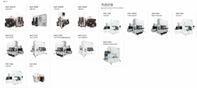
Please, Log in or Register to view URLs content!
I still think AMEC offers and focus more on the cutting edge tools while Naura offers more the working horse stuff of a semiconductor fab.
 

tokenanalyst

Brigadier
Registered Member

Peking University releases OpenPARF, an open source layout and routing framework for large-scale FPGA chips​


Field Programmable Logic Gate Array (FPGA) chip is a reconfigurable semi-custom integrated circuit, which can be programmed in hardware according to the needs of users to achieve specific functions. FPGA is mainly used in many fields such as digital signal processing, communication, embedded system, image and video processing, network acceleration, artificial intelligence, etc., and has a wide range of applications.
In the past ten years, with the continuous development of semiconductor manufacturing technology, the industry has gradually improved the integration and systematization of FPGA chips, adding a large number of high-speed computing units, memory-level resources, and domain-specific accelerators. Integration and systematization pose greater challenges to EDA tools for FPGA chip design. How to improve the performance, efficiency, and flexibility of EDA tools to adapt to diverse on-chip computing resources has become one of the bottlenecks in FPGA applications.
In order to achieve this goal, the team of Lin Yibo, Department of Design Automation and Computing Systems, School of Integrated Circuits, Peking University/EDA Research Institute, Peking University, Wuxi, released an open source layout and routing framework for large-scale FPGA chips - OpenPARF. Its main features are as follows:
High quality. OpenPARF integrates the most advanced placement and routing algorithms in the current academic world, and can complete placement and routing tasks on large-scale FPGA chips, and the solution quality and operating efficiency have reached the international leading level.
 High performance. OpenPARF fully exploits the parallelism of algorithms and uses GPUs to achieve heterogeneous parallel acceleration, which can greatly reduce the running time of layout and routing compared with traditional tools.
 Integrate with deep learning tools. OpenPARF is implemented based on the deep learning framework PyTorch, using C++/CUDA/Python hybrid programming, which combines the efficiency of C++/CUDA and the flexibility of Python. The code is flexible and easy to use, and it is convenient to integrate artificial intelligence algorithms.

1690925996717.png

Please, Log in or Register to view URLs content!
 

latenlazy

Brigadier
I'm not an expert but it seems individual transistors switch at similar rates. Voltage transients are measured in the picoseconds between current FinFETs and next generation nanosheets.

Please, Log in or Register to view URLs content!

I believe clock rate limitations are not on the transient decay rate but on the thermal capacity.
The “correct” answer here is that clockspeed is not the measurement of switching speed *but* the measurement of how many switch operations you’re doing per unit of time. That’s why the measurement is *frequency*. You can drive computations faster by making your transistors do more switch operations in a unit of time and in theory at least faster switch speeds means it’s easier to squeeze in more switch operations *but* there’s also probably limitations with material constraints and also with the overall processor architecture since you actually have to be able to drive the current needed to drive more switch operations.
 

tokenanalyst

Brigadier
Registered Member

Zhang Zhiyong-Peng Lianmao joint research group has made important progress in the field of advanced node carbon-based integrated circuits​


The main way integrated circuits have evolved is by shrinking transistor size to increase performance and integration while reducing power consumption and manufacturing costs. With the gradual application of 5 nm and below node CMOS technology in commercial VLSI, the continued scaling of silicon-based transistors faces limitations from power consumption, cost and even physical limits. In order to continue to promote the development of integrated circuits, academia and industry have conducted extensive exploration and in-depth research on the core materials, device structures, and system architectures of future electronics. Among them, the most concerned method is to use ultra-thin, high-carrier-mobility semiconductors to build CMOS devices with better scalability and higher performance than silicon-based transistors. Carbon nanotube transistors have shown the potential to outperform commercial silicon-based transistors and are therefore expected to be used in future digital integrated circuit applications. However, most of the research work has focused on the reduction of the gate length of the device, so the potential of carbon nanotube transistors in terms of integration level has not really been demonstrated. The gate pitch (CGP) is the key feature size to measure the integration density of transistors. However, the gate pitch of transistors based on carbon nanotubes or other low-dimensional semiconductors currently shown in academia is generally large (generally greater than 400 nm), which cannot truly achieve high density. integrated. Therefore, it is of great significance for the standardization of carbon nanotube technology to explore the performance advantages of carbon nanotube transistors and circuits compared with mainstream silicon-based technologies under the limited gate spacing, and to formulate the technical indicators of the first generation of carbon nanotubes.
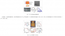
The Zhang Zhiyong-Peng Lianmao joint research group of the School of Electronics, Peking University, the Carbon-based Electronics Research Center, and the Key Laboratory of Nano-device Physics and Chemistry of the Ministry of Education demonstrated for the first time a 90 nm node transistor and circuit based on arrayed carbon nanotubes. The possibility of further shrinking base transistors to the 10nm node. The research group used the previously developed wafer-level high-density and high-purity semiconductor (~ 300 CNT/μ, 99.9999%, Science 368, 850, 2020) carbon nanotube array film to reduce the gate length of the transistor and the length of the source-drain contact (contact Length L con = 80 nm, gate length L g = 85 nm), a carbon nanotube field effect transistor with a CGP of 175 nm was prepared, the on-state current reached 2.24 mA/μm, and the peak transconductance g m was 1.64 mS/μm, Performance exceeds silicon-based commercial 45 nm node devices (Figure 1).

1690926491196.png
Please, Log in or Register to view URLs content!
 

BlackWindMnt

Captain
Registered Member
The “correct” answer here is that clockspeed is not the measurement of switching speed *but* the measurement of how many switch operations you’re doing per unit of time. That’s why the measurement is *frequency*. You can drive computations faster by making your transistors do more switch operations in a unit of time and in theory at least faster switch speeds means it’s easier to squeeze in more switch operations *but* there’s also probably limitations with material constraints and also with the overall processor architecture since you actually have to be able to drive the current needed to drive more switch operations.
Is that why they invented/designed hyper threading in cpu? So they can push a bit more operation per tick.
 

tokenanalyst

Brigadier
Registered Member
Depends on perspective. All those companies that you talked about are private companies in capitalist states whose only rule is the jungle rule, one kills everyone else.

China is not capitalist state, a private company's success means NOTHING to the general public if not serving the good for the whole population. The only judgement of any company's value is if it promote the industrial and technical compability of the WHOLE country. One super powerful company in a monopoly position is certainly against that purpose.

Example, there were two railway companies (south and north) in China. They competed one another in lowering prices abroad. They are essentially bleeding China's treasure by firecefully beating each other. Their own good is bad for the country. Therefor we saw them being merged into one recently. They are all state companies, so it is easier to handle. I am not advocating same dealing of Huawei, far from it. But certain limit must be set so it is not Chinese company killing another Chinese company.

Huawei is NOT a national hero, it is a commercial company whose primary aim is its own profit, which is not always in line with the national interest.
Sometimes the national interest/security doesn't pay the bills so a balance is needed. In the business world you have to be competitive or die, Huawei doesn't only have to compete against others Chinese companies but also with international companies that are as aggressive or even more as they are, is a jungle, all of that while fighting a technological guerrilla warfare against uncle sam, granted much like in the second Indochina wars they are receiving as much support from the government as possible but still is tough fight.
I don't think a lot of Chinese see Huawei as a national hero but more like image of a more competitive/advance China and now I think is more a symbol of resistance against a more powerful power.
My critique against Huawei and many others in China is why they didn't see this coming and prepare themselves for the storm? Huawei considered getting into semiconductors manufacturing almost a decade ago but they decide against, they didn't localize their supply chain until the last moment, back in the day Huawei and their bosses pretty much where the most industrialist trade liberal pro-globalization Chinese company ever. The US destroyed all that with the stroke of a pen and now the Chinese government has to intervine to lend some support to them.​
 
Status
Not open for further replies.
Top