Maybe leave out voiding the IP part as it might cause unexpected consequences on China's own IP. Concentrate on the breach of contract part and sue for damages. Pleading force majeure should be rejected as it is willful act of sabotage.From @WTAN and @tokenanalyst previous post about a rumor of SMEE SSA800 benchmarking against ASML NXT 2000i, I think we can say that the news can be true as YMTC is planning to sue ASML for damages incur with a possibility of ASML being sanction by China. The Chinese will not do this unless there is an alternative ready. From my mentor @Oldschool
[/HEADING]
[HEADING=3]OldschoolJunior Member
Registered Member
13 minutes agoNew
Counterstrike against ASML maybe on the way.
The latest I heard is YMTC president said the company will sue ASML and ask it buy back all the ASML DUVs in China that it will refuse to provide service. If ASML refuse to buy back and refuse to provide service, YMTC would ask the court to void all ASML DUV IPs in China.
Hopefully the court would void ALL ASML IP in China including the EUV because it accepted payment and refuse to deliver.
Samething with US and Japanese equipments, Hopefully the court would void them all as well
After that, domestic equipments could come out without fear of being sued.
Anything goes.
You are using an out of date browser. It may not display this or other websites correctly.
You should upgrade or use an alternative browser.
You should upgrade or use an alternative browser.
Chinese semiconductor industry
- Thread starter Hendrik_2000
- Start date
- Status
- Not open for further replies.
Is possibility for China to do a amendment that if a technology is prohibited from being sold inside China like EUV for example will lose its patent and/or IP protection status. China should make clear to Western country that the logic behind patents is to advance progress not to stop progress.Maybe leave out voiding the IP part as it might cause unexpected consequences on China's own IP. Concentrate on the breach of contract part and sue for damages. Pleading force majeure should be rejected as it is willful act of sabotage.
Thanks bro I share the same sentiment with China innovating it may bite them back in the future, BUT looking from economic point of view, what will happen to ASML? Samsung, SK Hynix, Intel and Micron all had suffered huge loses and may cancel their order of EUVL? Samsung plan of Counter Cyclical manner during a downturn is outdated due to competition from the Chinese. I may think TSMC may also decided to halt it's expansion plan due to economic uncertainty. I think ASML will be hit a triple whammy by restricting sales to China due to security concern, a dismal economic outlook and the competition from SMEE and other Chinese tech company.Maybe leave out voiding the IP part as it might cause unexpected consequences on China's own IP. Concentrate on the breach of contract part and sue for damages. Pleading force majeure should be rejected as it is willful act of sabotage.
The main factory building of the third phase of Cansemi Semiconductor project will be capped and the process equipment will be moved in early next year

CanSemi’s official Weibo news showed that the main factory building of CanSemi’s new 12-inch integrated circuit analog characteristic process production line project (Phase III) was successfully capped. The third phase of the project will enter the construction stage of clean room and power installation, and it is expected that the process equipment will be moved in early next year.
Yuexin Semiconductor said that since the start of the third phase of the project, more than 2,500 construction workers have entered the site, the earthwork processing volume is about 160,000 cubic meters, and 260,000 cubic meters of concrete pouring have been completed, achieving a total of 2.1 million safe working hours. The total construction area of the project is about 820,000 square meters. In addition to the main plant, it also includes power plant, diesel engine room, wastewater treatment station, bulk gas station and other areas.
According to reports, on the basis of the first and second phase projects, the third phase of the project will continue to target the fields of industrial electronics and automotive electronics, and focus on the improvement of the quality specifications of the process platform on the basis of the existing technology platform; firmly grasp the industrial terminals of the Guangdong-Hong Kong-Macao Greater Bay Area Advantages, in-depth cooperation with domestic industrial chip end users, automotive terminal manufacturers and first-tier suppliers, to provide customers with better and higher quality products. CanSemi will continue to accelerate the construction of the third-phase project with a total investment of 16.25 billion yuan, and strive to be fully completed and put into production in 2024.
Espressif Systems achieved double growth in revenue and net profit in the first half of the year.
Espressif Technology released the 2023 semi-annual report. In the first half of the year, the company achieved operating income of 667 million yuan, an increase of 8.66% over the same period last year; the net profit attributable to the owners of the parent company was 645.703 ten thousand yuan, a year-on-year increase of 2.05%.
Espressif Technology pointed out that the company’s net profit growth in the current period is mainly affected by four factors, one is the growth of operating income, the other is the stability of gross profit margin, the third is the increase in research and development expenses, and the fourth is the increase in the amount of income tax deductions.
After years of technology accumulation and product innovation, Espressif Technology has a lot of technology accumulation and continuous innovation capabilities in the field of embedded MCU wireless communication chips. Both have self-developed core technologies.
Espressif's products take "processing + connection" as the direction. In the field of the Internet of Things, there are currently a variety of IoT chip product lines. "Processing" takes MCU as the core, including AI computing; "connection" takes wireless communication as the core, and currently includes Wi-Fi, Bluetooth, Thread, and Zigbee technologies, and the product boundary has expanded to the Wireless SoC field.
Ziniu Yidong invested 3 billion yuan to build an IC core component R&D and industrialization base.
Wuhan East Lake High-tech Zone and Ziniu Yidong Technology Co., Ltd. held a signing ceremony, and Ziniu Yidong integrated circuit core component R&D and industrialization projects settled in Optics Valley.
With a total investment of 3 billion yuan, Ziniu Yidong plans to invest in the construction of an integrated circuit core component R&D and industrialization base in the East Lake High-tech Zone, which will attract a number of domestic and foreign high-quality industrial chain enterprises to land in the later stage.
According to China Optics Valley news, the Ziniu Yidong project will build the largest domestic component R&D, production and verification platform in Optics Valley, which is of great strategic significance to further improve the integrated circuit industry chain in the high-tech zone and help build a world-class integrated circuit industry cluster .
In 2021, Ziniu Yidong was established . It is an enterprise in the field of localized semiconductor equipment components. It has supplied more than 100 core components such as electronic-grade seals, metal parts, Si/SiC parts, graphite parts, and quartz parts to domestic chip manufacturers. There are more than 600 kinds of parts and components under research.
X-ray online full inspection technology improves IGBT yield
In the post-Moore era, the size of transistors is approaching the limit of the physical volume of atoms, and applications such as 5G, autonomous driving, artificial intelligence, and the Internet of Things are developing rapidly, requiring smaller chip sizes, lower power consumption, and stronger performance, which will inevitably lead to packaging The process is becoming more and more complicated, the reliability of the chip is reduced, it is easy to fail, and the yield rate is reduced. It can be solved from two aspects, one is that the chip material uses SiC and other materials, and the other is the chip packaging process.
1. XG5500 power device - welding defect
The XG5500 equipment mainly detects welding defects of power devices. It adopts 2D/2.5D online full inspection method. It is generally used in the production process of products. It can be applied to industrial-grade, consumer-grade, and automotive-grade IGBT modules. It is detected through online full inspection. Welding point defects, NG selection for defective products that do not meet the inspection items, to prevent defective products from flowing into downstream terminals.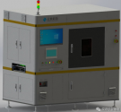
2. XG5500 discrete device - line defect
The XG5500 dedicated model for discrete devices exclusively developed by Zhengye Technology has two highlights:①The detection efficiency is very highIt adopts the matrix image acquisition of the whole plate, no need to pull the coil material, has a CCD vision positioning system, and the robot automatically loads the material. It takes 3 minutes (3000pcs) to detect the 7-inch material plate, and the misjudgment rate reaches 3‰, basically can achieve 0 error Sentence;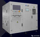
Fast flat-panel CT (online full inspection)
Fast flat-panel CT equipment is mainly aimed at car-level chips, which can realize online full inspection. Automotive-grade chips have high requirements for air bubbles, especially for new energy manufacturers. The fast flat-panel CT of Zhengye Technology is a full 3D online automatic imaging and analysis, which can be used for online detection and offline analysis. Through CT tomography technology, it can solve the inspection of laminated solder joint defects that cannot be realized by traditional 2D/2.5D equipment, such as Open, HIP, QFP/LGA, etc. In terms of efficiency, it can detect an IGBT sample in 1~1.5 minutes, and the accuracy can be as low as 2μm.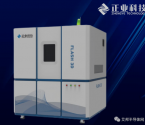
SICC say it has been delivering 6-inch conductive SiC substrate wafers to customers (probably since May) and has developed capability to mass produce 8-inch wafers
they expect to reach 300k wpy long before the originally 2026 timeline.
They've now done environmental studies to increase production to 960k wpy at their Lingang plant, so that's a huge in production
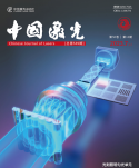
Homogenization of Lithography Illumination: The combination of microcylindrical mirror array and integrating rod works well.
The cover shows a light dodging unit of a lithography machine illumination system consisting of a single-row plano-convex microcylindrical lens array (PCMCLA), a three-piece condenser lens group, and a rectangular integrating rod. After the incident ring-shaped illumination beam is divided and expanded by PCMCLA and condenser lens group, it is superimposed at the incident end of the integrating rod to form a stripe-shaped spot with uniform distribution of intensity in the horizontal direction; after being homogenized by the integrating rod, a rectangular shape is finally formed at the exiting end of the integrating rod Uniform light field. The relay mirror group behind the homogenization unit images the light field onto the reticle. The uniform light unit is optimized based on the evaluation function of the cosine distribution of the light direction. The uniform light effect is better than the design based on the root mean square evaluation function of the traditional diffuse spot, and combines the advantages of the integrating rod and PCMCLA to meet the illumination uniformity of KrF lithography. requirements while taking into account system length and manufacturability.
- Status
- Not open for further replies.


