Chinese semiconductor industry

Status
Not open for further replies.

tokenanalyst

Brigadier
Registered Member
Since you know fair amount about these different kind of Deposition tools, can you elaborate on which kind of Deposition is used when? For example, I do know, MOCVD is used for LED Display but what about PVD, SACVD, PECVD, WCVD, ALD and the rest?
Is complicated, you can write entire books about this sh*t. Will depend on the material, how the film will be deposit, the rate of deposition, the temperature required, the chamber pressure, the desirable thickness of the layer, for what process, how is going to be etched and so on.

PVD includes sputtering, thermal deposition and other methods that physically transfer material from a source to a substrate, mainly good for coating metals and certain compounds like nitrides. Very high temperature and require very high vacuum.
Please, Log in or Register to view URLs content!

CVD use chemical reactions to deposit a thin film in the substrate.

PECVD is just using plasma to excite the gas molecules to enhanced the reaction, I think is mostly use when you want to deposit materials without rising too much the temperature. Dielectrics like SIO2

Please, Log in or Register to view URLs content!

SACVD is more use in high temp and pressure applications. I think offer higher rate of deposition.
Please, Log in or Register to view URLs content!

W-CVD the W stand for tungsten, depositing tungsten using the chemical reaction of a tungsten compound gas.

Please, Log in or Register to view URLs content!

ALD is chemical deposition but depositing an atomic thick layers, you can deposit atomic thin layers of metals, oxides and so on depending on the technique plasma enhanced ALD or thermal ALD

Please, Log in or Register to view URLs content!

then you have low preasure chemical deposition LPCVD

Please, Log in or Register to view URLs content!


Epitaxial deposition to grow crystals structures in a substrate with minimal defects.

Please, Log in or Register to view URLs content!

HDP-CVD high density plasma chemical deposition for thicker films at low temperatures.

Jiaxin Semiconductor wants to enter that field.

Please, Log in or Register to view URLs content!

copper electroplating

Please, Log in or Register to view URLs content!

For GAA transistors this paper cite the use of RPCVD.
1689807224707.png
Please, Log in or Register to view URLs content!
 

FairAndUnbiased

Brigadier
Registered Member
Since you know fair amount about these different kind of Deposition tools, can you elaborate on which kind of Deposition is used when? For example, I do know, MOCVD is used for LED Display but what about PVD, SACVD, PECVD, WCVD, ALD and the rest?
PVD - physical vapor deposition. Either evaporation to directly vaporize a compound, sputtering (using Ar+ ions to blast off pieces of a metal target that fly off onto your substrate) or pulse laser deposition (sputtering with a pulsed laser instead of ion beam). Evaporation is used for OLED mostly, sputtering is used for mostly metals, PLD is used for mostly simple inorganic compounds like oxides or nitrides.

CVD - multiple variations. simple CVD: spray an organometallic gas phase compound containing target film compound on a heated wafer. The molecule dissociates on the hot wafer. You now have a film. To enhance this process, you might want to excite the gas with plasma first, or have multiple reactants (such as an oxygen source for oxides) etc.

ALD - atomic layer deposition. Similar to CVD but with 2 steps: one is a surface prep step, the other is the deposition step. This makes it highly controllable to atomic precision. in exchange deposition rates are slow.
 

Fredrik

New Member
Registered Member
Google's Bard:

"Yes, you are correct. YMTC, a Chinese semiconductor company, announced in August 2022 that it had started mass production of its 232-layer 3D NAND flash memory. This was a significant milestone, as it made YMTC the first company in the world to mass produce 200+ layer NAND flash.

YMTC's 232-layer NAND flash is based on the company's Xtacking 3.0 architecture, which allows for the stacking of multiple NAND layers in a more efficient way. This results in a higher storage density and improved performance.

YMTC's 232-layer NAND flash is currently being used in a variety of applications, including smartphones, tablets, and solid-state drives. The company expects to see increasing demand for its 232-layer NAND flash in the coming years.

The 128-layer NAND that you mentioned is a previous generation of NAND flash that is still in use today. It is less dense and less performant than YMTC's 232-layer NAND, but it is also less expensive.

As the demand for storage continues to grow, we can expect to see even higher-density NAND flash being developed in the future. YMTC is a leading player in this field, and it will be interesting to see what they come up with next."
 

tokenanalyst

Brigadier
Registered Member

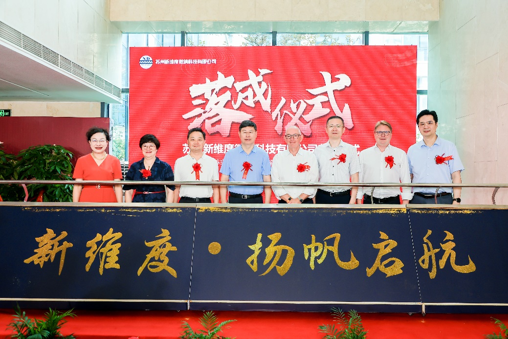
Suzhou New Dimension settled in Suzhou Industrial Park, focusing on the industrialization of nanoimprint technology​


1254750994867.5217304733714196.46533.png

Source: SIP Technology Leader
According to Dr. Luo Gang, general manager of New Dimension, New Dimension has inherited the nanoimprint technology system of Academician Liu Zhongfan and Professor Lars Montelius of Sweden, and is one of the world's main nanoimprint technology routes. On this basis, New Dimension Company further develops related technologies, combines with downstream specific applications, improves production efficiency and effectively reduces production costs, and brings customers products with price advantages. New Dimension will focus on the field of AR/VR products for a long time, continue to improve its own market competitiveness, and strive to bring low-cost and high-experience AR/VR interactive products to the society.
According to New Dimension's official news, Professor Lars Montelius, the European founder of nanoimprint technology, believes that nanoimprint has great technical potential and capabilities in solving AR/VR products. He hopes that New Dimension can stay true to its original intention and realize consumer-oriented AR/VR products

Please, Log in or Register to view URLs content!
 

tphuang

Lieutenant General
Staff member
Super Moderator
VIP Professional
Registered Member
why despite abundance of Chinese chip improvement, the demand for Nvidia AI GPUs are still off the hook
Please, Log in or Register to view URLs content!
10x demand for AI in half a year

Please, Log in or Register to view URLs content!
high speed ETC (electronic traffic control?) using Loongson chips? Anyways, hopefully we see more success like this for not just LoongArch desktop CPUs but also industrial chips
 

ansy1968

Brigadier
Registered Member
Please, Log in or Register to view URLs content!

TSMC delays U.S. chip plant start to 2025 due to labor shortages​


@tphuang sir.
Bro, my take it will be delayed until 2026, when a new Taipei administration take over and the 2nm chip start production in Taiwan.

And also due to economic uncertainty, the Arizona FAB will only produce the 5nm chips not the 3nm.
 
Status
Not open for further replies.
Top