Chinese semiconductor industry

Status
Not open for further replies.

tphuang

Lieutenant General
Staff member
Super Moderator
VIP Professional
Registered Member
Please, Log in or Register to view URLs content!
Zhejiang starshine semi was formed in January 2022 with the goal of developing RF front end filter & module technology. SAW & BAW filters, duplexers & such

In April, signed deal to produce 120k wafers per year of 5G wafers

With recent news, it seems like things are coming together all along 5G. I think they might end up going from having little presence on upstream supply chain to dominating upstream supply chain in a short time, because they are the downstream companies & cutting off raw materials to upstream suppliers. And they are building up production quickly with many companies at the same time.
 

tokenanalyst

Brigadier
Registered Member

Semiconductor Quantity Testing Equipment Manufacturer, Zhongan Semiconductor Completed Hundreds of Millions of A+ Rounds of Financing​


Recently, Nanjing Zhongan Semiconductor Equipment Co., Ltd. ("Zhongan Semiconductor") completed hundreds of millions of yuan in A+ round financing, led by Fengyuan Capital, and co-invested by Co-Stone Capital, SMIC Juyuan, and Yuanhe Puhua.
Founded in 2020, Zhongan Semiconductor focuses on semiconductor quality inspection equipment. Its main products include wafer geometry measurement equipment, wafer particle defect inspection equipment, etc. Among them, the wafer geometric shape measurement equipment mainly performs non-contact optical interferometry for wafer warpage, flatness, thickness, film stress and other parameters; the wafer particle defect detection equipment uses the principle of light scattering and uses high-power deep ultraviolet technology to provide non-contact optical detection of wafer particle defects.
According to news from Fengyuan Capital, Zhongan Semiconductor products are mainly used in large silicon wafer production, wafer manufacturing, equipment research and development, advanced packaging and other fields. The core technology covers precision opto-mechanical, deep ultraviolet, high-speed cameras, etc., and has self-developed core algorithms. The performance of the equipment is internationally leading. At present, it has been highly recognized and repeated orders by many leading customers, and through technical iterations, it can meet customer customization needs. The future business is expected to continue to increase.
In March 2020, the Zhongan Semiconductor Project signed a contract with Nanjing Jiangbei New District. According to news at the time, the Zhongan Semiconductor project was mainly to develop flatness and three-dimensional shape testing equipment for semiconductor silicon wafers, and was engaged in the development of flatness and three-dimensional shape testing equipment for 200mm and 300mm silicon wafers.

Please, Log in or Register to view URLs content!
 

tphuang

Lieutenant General
Staff member
Super Moderator
VIP Professional
Registered Member
tom's hardware reporting on YMTC
Please, Log in or Register to view URLs content!


where they are shocked to find out that YMTC start production of 128 layers using XTacking 3.0 tech. Makes all the sense in the world to me given that AMEC tools can only do 128 layers right now

He seems to be unable + unwilling to figure out that YMTC can just replace American tools with domestic ones
 

gelgoog

Brigadier
Registered Member
Yeah. The journalist does not seem to know that the US sanctioned deliveries of tools capable of 128 layers and over (inclusive).
So unless they use string stacking they cannot even make 128 layers NAND with those tools.
YMTC right now puts the memory layers in one wafer, and the logic on another wafer, then slaps them together.

YMTC is quite likely using Chinese tools capable of 128 layers.
 
Last edited:

tokenanalyst

Brigadier
Registered Member

Haixi Communication|Invested 100 million yuan in the cross-border layout of silicon carbide modules​


On July 19, Haixi Communications, a company listed on the Beijing Stock Exchange, issued an announcement saying: Based on the company's strategic planning, combined with market development prospects and business layout, it plans to use its own funds to increase the capital of its wholly-owned subsidiary Haixi Intelligent Technology (Zhejiang) Co., Ltd. by 100 million yuan to develop silicon carbide module modules, new energy related products and other businesses.
It is understood that the company previously signed the "Strategic Cooperation Framework Agreement" with Suzhou Chenlong Digital Technology Co., Ltd., a wholly-owned subsidiary of Suzhou Chenlong Holding Group Co., Ltd., on June 16, 2023. The company has established a long-term and stable strategic partnership through the introduction of Chenlong Digital, and has developed silicon carbide modules and new energy storage businesses to drive the diversified development of the industry and promote the company's high-quality and sustainable development.

Silicon carbide module modules can be applied to energy storage equipment. The company plans to invest in the construction of silicon carbide module modules and energy storage equipment projects. The construction period is about 24 months (including plant construction and equipment procurement), and new building such as module workshops, cell workshops, integration workshops, and raw material warehouses. After the project is completed, it will become an integrated large-scale industrial base that provides products such as module modules, batteries, battery modules, and energy storage system integration.

The above-mentioned business companies have completed the preliminary research, and the follow-up companies will carry out businesses such as silicon carbide module modules and new energy- related products. Chenlong Digital will provide support for the company's new business development and implementation, including but not limited to human and technical support.

Please, Log in or Register to view URLs content!
 

tokenanalyst

Brigadier
Registered Member

The team of Professor Zhu Jiaqi from Harbin Institute of Technology: Research progress on the band structure and physical properties of terminal diamond.​


Advanced fields such as 5G communication, energy Internet, new energy vehicles, and quantum technology have put forward new and higher requirements for the performance of semiconductors. The fourth-generation semiconductor diamond is known as the " ultimate semiconductor " because of its excellent physical and chemical properties, and is considered to be the most ideal material for the preparation of next-generation high-power, high-frequency, high-temperature and low-power loss electronic devices. The technical bottleneck of shallow n-type doping hinders the development of diamond semiconductor applications to a certain extent. The research on surface termination provides a new strategy for the development of diamond functionalization .Diamond has realized important applications such as field-effect transistors, Schottky diodes, solar-blind ultraviolet detectors, electron emission devices, and near-surface color center control through surface termination. The mechanism of surface termination is inseparable from its energy band structure characteristics. This paper summarizes the energy band research methods of several common terminals, analyzes the structural characteristics of their energy bands, introduces the mechanism of their function in combination with the characteristics, and makes a summary and prospect.
MBXY-CR-a7b31f88a6cc35fdf98917ffe96c22d2.png
 

tokenanalyst

Brigadier
Registered Member
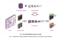
AI for lithography

Lithography dead point detection method based on pre-trained VGG11 model​

Lithography Hotspot Detection Method Based on Pre-trained VGG11 Model

Abstract
Results and Discussions In this study, ICCAD 2012 benchmark suite is used for model training and model tests. The ICCAD 2012 benchmark suite contains five subsets. According to the data-balance method, non-hotspot data are randomly sampled in the training data of the ICCAD 2012 benchmark suite. The randomly sampled non-hotspot data and all hotspot data constitute a complete training dataset, and the number of training data in the training dataset is 5054. The model test data are the five test datasets in the ICCAD 2012 b enchmark suite. With the pre-trained VGG13, VGG16, and VGG19 models as references, VGG model comparison experiments are conducted. As shown in Fig. 5 and Table 2, the comparison results indicate that the comprehensive performance of the model obtained by the propo sed method is better, and the average accuracy, recall, precision,andF 1 score of the model reach 98.9%, 98.2%, 89.5%, and 93.3%, respectively. In addition, the hotspot detection method based on the pre-trained VGG11 model requires a shorter model training time of only 279 s. The improvement of the model performance and model training time helps to improve the efficiency of hotspot detection. Compared with the hotspot detection method based on the pre-trained GoogLeNet model and the pre-trained VGG16 model, the results show that the proposed method has better comprehensive model perform ance. As shown in Fig. 6 and Table 4, on the premise that the hotspot detection has a considerable recall, the proposed method can significantly improve the precision and F 1score. Tests are carried out to release convolutional layers with different numbers for model training, and the results show that the release of the convolutional layers has a slight effect on the model performance of the proposed method.

1689783464602.png

Please, Log in or Register to view URLs content!
 

tphuang

Lieutenant General
Staff member
Super Moderator
VIP Professional
Registered Member
Please, Log in or Register to view URLs content!

Most important of all, China's share of ASML net system sales has grown from 8% in Q1 2023 to 24% in Q2 2023. Eric Chen, DIGITIMES Research analyst, believes that ASML has sped up shipment to China – now its third largest market.

Regarding the recent export controls announced by the Dutch government toward China, the ASML CEO noted that the final ruling "was more or less in line with what we communicated about a quarter ago," reiterating that the regulations, effective per September 1, dealt with NXT:2000i and subsequent models of DUV immersion systems.

definitely stocking up with some early deliveries before the sanctions hit. Look like ASML itself has anticipated the sanctions on maintenance & servicing of more advanced models. My guess is that it has probably worked with SMIC to deal with the consequences of that. Given that SMIC has managed to keep SMSC going all alone with Lam/Amat equipment, it will need to do that here also.
 

Wahid145

New Member
Registered Member
AMEC and Piotech are collaborating in deposition, AMEC is a investor of Piotech.

Naura has made a name to themselves in physical vapor deposition, sputtering, TSV deposition, advanced packaging and oxide deposition.
LeadMicro has made their entire business around Atomic Layer Deposition, high-k materials, depositing atomic thin layers of metals and oxides.
AMEC main business is MetalOrganic deposition and they are now the only player in China that sells Tungsten chemical deposition equipment.
Piotech is the only player in China with sub-atmospheric chemical deposition.

Of course they have overlapping businesses but everyone is trying to get their own niche market.
Since you know fair amount about these different kind of Deposition tools, can you elaborate on which kind of Deposition is used when? For example, I do know, MOCVD is used for LED Display but what about PVD, SACVD, PECVD, WCVD, ALD and the rest?
 

tphuang

Lieutenant General
Staff member
Super Moderator
VIP Professional
Registered Member
Since you know fair amount about these different kind of Deposition tools, can you elaborate on which kind of Deposition is used when? For example, I do know, MOCVD is used for LED Display but what about PVD, SACVD, PECVD, WCVD, ALD and the rest?
MOCVD is also used to grow GaN epitaxy on substrates

ALD is used for PV cells
 
Status
Not open for further replies.
Top