once you have immersion you dont need 157nm.157nm was given up due to many technical factors that were not able to overcome (for 1, very difficult to do immersion).
You are using an out of date browser. It may not display this or other websites correctly.
You should upgrade or use an alternative browser.
You should upgrade or use an alternative browser.
Chinese semiconductor industry
- Thread starter Hendrik_2000
- Start date
- Status
- Not open for further replies.
there seems to have unresolved photoresist and len problems for 157nm lithography.once you have immersion you dont need 157nm.
Thos is what Googles AI Bard says about the article:This site is locked tight, but maybe someone here knows more about it
"Digitimes Asia reported on July 17, 2023 that China-developed AI chips have entered the 7nm and below era. This is a significant development, as 7nm is the most advanced process node for AI chips currently available. The move means that Chinese AI chipmakers are now on par with their global counterparts in terms of technology.
The report cited sources from the AI chip supply chain who said that the manufacturing of China-developed AI chips at the 7nm node and below is being carried out by several companies, including Semiconductor Manufacturing International Corporation (SMIC), HiSilicon, and Cambricon. These companies are all working to develop their own 7nm AI chips, and some of them have already started to sample their products to customers.
The development of 7nm AI chips is important for China's AI industry, as it will allow Chinese companies to develop more powerful and efficient AI models. This will give them a competitive edge in the global AI market, which is expected to grow rapidly in the coming years.
Here are some of the benefits of using 7nm AI chips:
- They are more powerful and efficient than previous generations of AI chips.
- They can be used to train and run more complex AI models.
- They can be used in a wider range of applications, including self-driving cars, facial recognition, and natural language processing.
If that's all then it doesn't look like anything we haven't known for several months now. I suppose now we are going to look to see what Huawei might introduce for a new AI chip this year, considering that the Ascend 910 is already four years old at this point and is going up against the likes of H100s.Thos is what Googles AI Bard says about the article:
"Digitimes Asia reported on July 17, 2023 that China-developed AI chips have entered the 7nm and below era. This is a significant development, as 7nm is the most advanced process node for AI chips currently available. The move means that Chinese AI chipmakers are now on par with their global counterparts in terms of technology.
The report cited sources from the AI chip supply chain who said that the manufacturing of China-developed AI chips at the 7nm node and below is being carried out by several companies, including Semiconductor Manufacturing International Corporation (SMIC), HiSilicon, and Cambricon. These companies are all working to develop their own 7nm AI chips, and some of them have already started to sample their products to customers.
The development of 7nm AI chips is important for China's AI industry, as it will allow Chinese companies to develop more powerful and efficient AI models. This will give them a competitive edge in the global AI market, which is expected to grow rapidly in the coming years.
Here are some of the benefits of using 7nm AI chips:
The development of 7nm AI chips is a significant milestone for China's AI industry. It shows that Chinese companies are now capable of developing cutting-edge AI technology, and it will help them to compete with global leaders in the AI market."
- They are more powerful and efficient than previous generations of AI chips.
- They can be used to train and run more complex AI models.
- They can be used in a wider range of applications, including self-driving cars, facial recognition, and natural language processing.
On the Huawei FinFet design, does anyone have more information on how it achieves better performance compared to GAA? This development is probably one of the more significant advancements for Chinese chips, given that GAA is the trend for sub-3nm nodes right now.
Why are Huawei, SMIC taking different approaches against US curbs?On the Huawei FinFet design, does anyone have more information on how it achieves better performance compared to GAA? This development is probably one of the more significant advancements for Chinese chips, given that GAA is the trend for sub-3nm nodes right now.
Amanda Liang, commentary; Willis Ke, DIGITIMES AsiaFriday 19 May 2023

Credit: DIGITIMES
China's tech giant Huawei and top semiconductor foundry SMIC apparently adopt different approaches against US chip curbs. The former has just announced its successful development of electronic design automation (EDA) tools for chips above 14nm process, while the latter has quietly removed 14nm process technology from its service list on its website. What messages are these two Chinese tech players sending through their recent actions? And what are their actual calculations?
At a recent annual financial report conference, Huawei's rotating chairman Xu Zhijun said that over the past three years the company has focused on developing homegrown development tools for hardware, software, and chips amid the lingering US restrictions, and has achieved localization of EDA tools for above 14nm chips and will complete comprehensive verifications this year.
This means that despite its IC design arm HiSilicon suffering a major setback from tough US trade curbs, the successful development of EDA tools for 14nm chips can be said to be a secure self-protection strategy against the risk of being completely cut off by the US in the future.
According to Xu, Huawei's 14nm EDA software, jointly developed with a Chinese EDA vendor, will be incorporated into HiSilicon's chip designs and will also be shared with its partners and customers.
Huawei has not confirmed whether it is also cooperating with China's top EDA developer Empyrean Technology, which specializes in both front- and back-end EDA process nodes for 28nm chips, a mature chip segment with massive applications and with the most capacity expansion momentum at Chinese foundry houses.
Judging from the R&D deployments by Huawei and Empyrean, it seems that they do not want 14/28nm chip designs to be dominated by competitors in Europe and the US and are trying hard to materialize China's autonomy at least in the midrange/mature process nodes.
Then what about SMIC? The foundry has been engaged in mass production of 14nm chips since late 2019, yet with only a single-digit revenue contribution ratio for its most advanced process technology. But it has symbolized SMIC's mass commercial production of FinFET process technology, marking an important first step toward advanced processes in China, though it cannot be on a par with TSMC and UMC in terms of yield rates.
With capital support from the China National Integrated Circuit Industry Fund, also known as the "Big Fund," SMIC's FinFET process advancement is not meant to pursue maximum profits, but to prioritize the import-substitution chips supply and then progress to 7/5nm chips.
SMIC has no other choice but to take its development of FinFET process technology underground, given the upcoming new restrictions on shipments of higher-end DUV machines from Dutch and Japanese suppliers later in 2023. The company has been denied access to EUV lithography equipment supplied by ASML since 2019.
At a recent quarterly earnings call conference, SMIC's co-CEO Zhao Haijun spoke frankly about capacity expansion deployments at its four major manufacturing bases in China. He said its Shenzhen plant has entered volume production of high-voltage driver chips, CMOS image sensor chips, and power electronics chips; its new fab in Tianjin, still under construction, will focus on analog chips and power management ICs (PMIC); and new capacity at fabs in Beijing and Shanghai is set for volume production of multiple chip solutions in the second half of 2023.
But Zhao remained tight-lopped about the current production of 14/12nm chips or development status of more advanced 7/5nm processes at its FinFET wafer fab that has been operational since May 2019. At the current stage, the advanced process base near SMIC's headquarters in Shanghai has become a taboo subject.
The removal of 14nm fabrication technology from SMIC's list of services on its website can be interpreted as a kind of practice designed to give face to the US government in line with its curbs. But it is highly probable that SMIC is eyeing the horizon for future development possibilities.
Chiplet is the way to go and Hisilicon may do the packaging by using SMIC N+1 8NM chips. I'm NO expert BUT after graduating from kindergarden what I learn is that 1+1 is greater than 1.If that's all then it doesn't look like anything we haven't known for several months now. I suppose now we are going to look to see what Huawei might introduce for a new AI chip this year, considering that the Ascend 910 is already four years old at this point and is going up against the likes of H100s.
5 days ago — Huawei, China's tech and chip design giant that has been put on the US's most restricted list, has been actively filing chiplet patents. Huawei ...
Last edited:
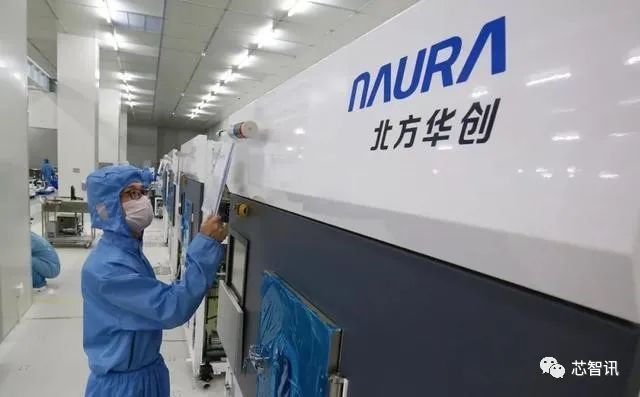
Naura unveils 1st domestic 12-inch bevel etch machine Accura BE, for the 1mm on the edge of 12-inch wafers to help with yields
Sounds like it has already entered mass production & being validated by several logic & memory fabs据介绍,在器件制造过程中,由于薄膜沉积、光刻、刻蚀和化学机械抛光等工艺步骤的大幅增长,在晶圆的边缘造成了不可避免的副产物及残留物堆积,这些晶边沉积的副产物及残留物骤增导致的缺陷风险成为产品良率的严重威胁,因此,越来越多逻辑及存储芯片等领域制造商开始重点关注 12 英寸晶圆的边缘 1mm 区域,从晶圆的边缘位置着手提高芯片良率。晶边刻蚀机作为业界提升良率的有力保障,其重要性日益凸显。
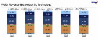
And how does DIGITIMES know that exactly? SMIC stopped reporting on their distribution of revenue by process. Last published breakdown is from Q3 2021.Then what about SMIC? The foundry has been engaged in mass production of 14nm chips since late 2019, yet with only a single-digit revenue contribution ratio for its most advanced process technology.

This is the last published breakdown of revenue by process from Q4 2021. I do not see how this jives with the claim that the most recent processes at SMIC only provide them with single digit revenue contribution. Especially when you consider that the advanced process yields must have improved as production went on. The last rumored claim we heard of was that the 14nm FinFET process had reached similar yields to TSMC's and 10nm FinFET was in mass production. Separately we have confirmed reports of SMIC's 7nm FinFET available in the wild.
It also fairly well known that SMIC had issues with yields with 28nm planar initially. And I would not be surprised if they got around to fixing that too. The reason for the lag with 28nm yields was due to Liang Mong-song wanting to go straight for FinFET instead of spending time improving yields on what he perceived to be old processes. But it is not like SMIC right now has anything better to do than improve existing processes is there.
Yields for what exactly? TSMC does not use EUV in processes above 7nm. There is no reason to expect that SMIC will eventually not reach similar yields to TSMC in 10nm and higher processes.But it has symbolized SMIC's mass commercial production of FinFET process technology, marking an important first step toward advanced processes in China, though it cannot be on a par with TSMC and UMC in terms of yield rates.
BS. SMIC clearly means to have competitive processes to the rest of the market whenever possible. As for 7/5nm that is being used for getting experience with advanced processes.With capital support from the China National Integrated Circuit Industry Fund, also known as the "Big Fund," SMIC's FinFET process advancement is not meant to pursue maximum profits, but to prioritize the import-substitution chips supply and then progress to 7/5nm chips.
The plan is that all those fabs are to be capable of 28nm planar transistor production. The article makes it seem like the plants are meant for even older processes. BS.At a recent quarterly earnings call conference, SMIC's co-CEO Zhao Haijun spoke frankly about capacity expansion deployments at its four major manufacturing bases in China. He said its Shenzhen plant has entered volume production of high-voltage driver chips, CMOS image sensor chips, and power electronics chips; its new fab in Tianjin, still under construction, will focus on analog chips and power management ICs (PMIC); and new capacity at fabs in Beijing and Shanghai is set for volume production of multiple chip solutions in the second half of 2023.
The Tianjin fab is meant to produce chips between 180nm and 28nm. Same deal for all other fabs they are building.
Does that that sound like analog chips and power management ICs?
What I am way more interested in, and I have seen other people share my skepticism, is why did SMIC go for building four new facilities with total combined production capacity of 340,000 300mm wafers per month. When their existing 300mm production is 113,000 wafers per month, with another 230,000 200mm wafers per month (equivalent to around 102,000 300mm wafers per month).But Zhao remained tight-lopped about the current production of 14/12nm chips or development status of more advanced 7/5nm processes at its FinFET wafer fab that has been operational since May 2019. At the current stage, the advanced process base near SMIC's headquarters in Shanghai has become a taboo subject.
The removal of 14nm fabrication technology from SMIC's list of services on its website can be interpreted as a kind of practice designed to give face to the US government in line with its curbs. But it is highly probable that SMIC is eyeing the horizon for future development possibilities.
So they are basically going to increase output by like 158%. The question is are they really going to do that or not?
Last edited:
NAURA's net profit in the first half of the year soared by 121.30%-155.76% year-on-year


On the evening of July 14th, North Huachuang, a leading domestic semiconductor equipment company, released its performance forecast for the first half of 2023. It is estimated that the operating income in the first half of the year will be 7.82 billion to 8.95 billion yuan, a year-on-year increase of 121.30%-155.76%; the net profit will be 1.67 billion yuan- 1.93 billion yuan, a year-on-year increase of 121.30%-155.76%; non-net profit deducted from 1.49 billion yuan to 1.72 billion yuan, a year-on-year increase of 130.90%-166.55%.
The previous financial report for the first quarter showed that North Huachuang’s operating income was 3.871 billion yuan, a year-on-year increase of 81.26%; the net profit attributable to the parent was 592 million yuan, a year-on-year increase of 186.58%; the deduction of non-net profit was 534 million yuan, a year-on-year increase of 243.59%. Based on this calculation, North Huachuang’s revenue in the second quarter is about 3.949 billion yuan to 5.079 billion yuan, a quarter-on-quarter increase of about 2.01%-31.21%; the net profit attributable to the parent is about 1.078 billion yuan-1.128 billion yuan, a quarter-on-quarter increase of 82.09%-90.54% ; Deduction of non-net profit of 956 million yuan to 1.186 billion yuan, a month-on-month increase of 79.03%-122.10%.
It can be seen that NAURA's performance in the second quarter still maintained a relatively large growth compared with the first quarter.
Regarding the growth of the overall performance in the first half of the year, North Huachuang said that it mainly benefited from the steady increase in the market share of the company's semiconductor equipment business and the continuous improvement in operating efficiency. The company's total operating income and net profit in the first half of the year both achieved year-on-year growth.
- Status
- Not open for further replies.
