You are using an out of date browser. It may not display this or other websites correctly.
You should upgrade or use an alternative browser.
You should upgrade or use an alternative browser.
Chinese semiconductor industry
- Thread starter Hendrik_2000
- Start date
- Status
- Not open for further replies.
The law of diminishing returns. At that point the Chinese will do almost everything themselves and because price is king in this world the Chinese to much of the dismay of the Americans could end even more embedded in the semiconductor supply chain than in the past because now they are an alternative supplier of materials, components, software and machinery. Be sure that a lot of Chinese supplier as they get big inside China they will promote their product outside of China.
This is an article from February 2023, but it perfectly encapsulates the attitudes of a very influential section of the US power elites when it comes to China and technology. If guys like that had their own way, one shouldn't even sell food to China because food is consumed by the "evil" members of the Communist Party who are hell bent on ensuring that China eclipses the United States as the largest economy in the world et al... And food is what allows them to live...
Here is an excerpt from the article:
If the Biden administration is ready to take more action as it relates to Huawei, will the same soon follow for SMIC? What about CXMT, another Chinese chip bellwether, and one that seems to fly under the radar compared to SMIC and YMTC? Like Huawei, SMIC is Entity Listed, but the current restrictions clearly aren’t enough. Even with a potential partnership with Huawei aside, SMIC just had a banner year and is doubling down on the production of mature chips. This shows a strategic misstep on the part of the U.S. government to focus restrictions on leading edge chips – leaving the door open for companies like SMIC to redirect its focus and keep its quest for market dominance in sight.
Do not be surprised when the day comes that 1950s era nodes and semiconductor related manufacturing equipment is banned from sales to China, or at least shrill calls for that to happen and most Democrats and Republicans will be in agreement for it...
Is already happening, with ACMR in South Korea, Naura in South East Asia and AMEC probably in the US.
The new land of Lite is completed in Wuxi, and another 70 million US dollars will be invested in the construction of 6-inch wafer production line
Lite’s new plot was completed in Wuxi. At the same time, Wuxi High-tech Zone and Lite Semiconductor (Wuxi) Co., Ltd. signed a strategic cooperation agreement for capital increase and production expansion projects.According to the agreement, the company plans to invest a total of US$70 million in the next five years (2023-2027), mainly investing in the construction of a 6-inch wafer production line.
Littelfuse Group is a world-leading multinational company in the field of circuit protection. Littelfuse Semiconductor (Wuxi) Co., Ltd. mainly produces circuit protection components, including 5-inch wafer product lines and packaging and testing production lines. It is a circuit protection product of Littelfuse Group. The largest production base.
According to the online information of Wuxi High-tech Zone, the new plot completed this time covers an area of 13.8 mu, with a total investment of 90 million US dollars.
Gechuang Dongzhi acquires the ownership of semiconductor EAP provider Feixunte in mainland China.
Gechuang Dongzhi has fully acquired the ownership of the source code of the Feixunte EAP software suite in mainland China , as well as the exclusive sales right and brand authorization. At the same time, focusing on the expansion of overseas markets, the two parties will join forces and work together to promote China's semiconductor intelligent manufacturing solutions to the world.
Founded in 2018, Gechuang Dongzhi focuses on the upgrading of intelligent manufacturing in the semiconductor industry. Its self-developed data intelligent products have successfully helped customers realize the process from silicon wafer, wafer manufacturing, packaging and testing, to finished product assembly, from multi-workshop, to Multi-factory production management, quality traceability and process optimization.
Festech was established in Hsinchu, Taiwan, China in 2001. It focuses on providing factory automation integration services and developing machine equipment automation EAP software. It is one of the best EAP software companies in the global semiconductor industry. It has served TSMC, UMC, Powerchip, Hua Semiconductor customers such as Bang Electronics, Changxin Storage, Hua Hong, and Silan Micro.
Maiwei plans to invest 3 billion yuan in the construction of pan-semiconductor equipment projects.
Suzhou Microway Technology Co., Ltd. announced that it plans to sign an "Investment Agreement" with the Management Committee of Wujiang Economic and Technological Development Zone to invest in the construction of the "Maiden Pan-Semiconductor Equipment" project, and independently develop and manufacture pan- High-end equipment in the semiconductor field, the total planned investment of this project is 3 billion yuan, and the planned land area is about 259 mu.
In recent years, relying on the high-speed and high-precision control technology, high-precision positioning technology and other technical advantages and customer base, and relying on years of research and development technology accumulation, Maiwei has successfully developed semiconductor packaging equipment and display panel equipment, and has achieved rapid development. , Semiconductor packaging-related products have been successfully imported into domestic mainstream packaging and testing manufacturers such as Sanan Optoelectronics, Changdian Technology, and Jiejie Microelectronics. The semiconductor packaging equipment and display panel equipment of Maiwei Co., Ltd. have been accepted by customers one after another, with stable operation and good performance.

Suzhou Microway Technology Co., Ltd. (hereinafter referred to as "Maywell") was established in September 2010. It is a high-end equipment manufacturer integrating mechanical design, electrical research, software development, and precision manufacturing. The company is oriented to solar photovoltaic, The three major industries of display and semiconductor, R&D, manufacturing and sales of intelligent high-end equipment, the main products include fully automatic solar cell screen printing production line, overall solution for heterojunction high-efficiency battery manufacturing, OLED flexible screen laser cutting equipment, Mini/Micro LED Wafer equipment, semiconductor wafer packaging equipment, etc.
Based on the three key technology platforms of vacuum, laser, and precision equipment, and adhering to the belief of realizing the localization of core equipment through independent research and development and technological innovation, Maiwei always takes the top level of the industry as the standard, continues to explore, and strives to become a subdivided industry in the pan-semiconductor field Benchmarking, promoting the progress of intelligent manufacturing technology.
The company's main product, solar cell screen printing production line, will rank first in the domestic market share from 2016 to 2022, and will rank first in the global market share from 2018 to 2022*.
Xuzhou Bokang appeared at the World Semiconductor Conference! Focus on photoresist research and development, and commit to independent and controllable supply chain.
It is understood that Xuzhou Bokang was established in 2010, the production base is located in Pizhou, Jiangsu, and the R&D center is located in Songjiang, Shanghai.
Xuzhou Bokang is a national high-tech enterprise integrating research and development, production and operation of high-end photoresists, photoresist monomers and photoresist resins. Xuzhou Bokang focuses on the independent research and development and production of photolithographic collagen materials to finished products, and has realized an independent and controllable supply chain from the localization of monomers, photoresist-specific resins, photoacids and final product photoresists.
At present, Xuzhou Bokang's product line covers 193nm/248nm photoresist monomer, 193nm/248nm photoresist, G line/I line photoresist, electron beam photoresist and other products. At present, 40+ high-end photoresist product series have been successfully developed, including a variety of electron beam glue, ArF dry photoresist, KrF positive and negative photoresist, I-line positive and negative photoresist and GHI ultra-thick Negative glue, used in multiple links of IC integrated circuit manufacturing, serving more than 100 customers.
The R&D team is strong and has rich photoresist professional capabilities
It is understood that Xuzhou Bokang is led by Mr. Fu Zhiwei, a representative of the 14th National People's Congress, a candidate for the National Major Talent Project, and an innovative and entrepreneurial talent from the Ministry of Science and Technology. It is composed of experts in lithography materials and lithography technology at home and abroad. At present, the company has more than 500 technicians, accounting for more than 70%. The front-line R&D team consists of more than 200 people, of whom masters and doctors account for more than 50%. They have rich professional capabilities in organic synthesis, polymer polymerization, and semiconductor-grade electronic-grade purification. They have systematically mastered the core technology of electronic-grade chemical production.
As of May 2023, there are 116 invention patents under review and 65 invention patents authorized.
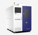
Microconductor Nano Releases 2 Major New Products: The First Generation iTronix® Series CVD Film Deposition Equipment
On June 29 , SEMICON China 2023, the world's largest and most influential semiconductor event, was kicked off in Shanghai. At the event site, Jiangsu Microconductor Nano Technology Co., Ltd. (stock code 688147 , referred to as " Microconductor Nano " ) presented two major new products and officially released the first-generation iTronix® series CVD film deposition equipment independently developed by the company. This marks another breakthrough in the field of semiconductor thin film deposition by Microconductor Nano, and it is also a key step for the company's diversified layout to activate new growth drivers.
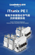
iTronix ® PE series plasma-enhanced chemical vapor deposition coating system can deposit different kinds of films, which can be applied to chip manufacturing in the fields of logic, storage, advanced packaging, display devices and compound semiconductors. At the same time, the new platform can be equipped with more reaction chambers to meet high production capacity requirements.

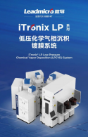
iTronix ® LP series low-pressure chemical vapor deposition coating system adopts specially designed reaction chamber and electrical software integration services. It is widely used in the fields of logic chips , DRAM chips , NAND chips , etc. -Development and application requirements of Si , SiO 2 , SiN and other thin film deposition processes.

As a leading enterprise in domestic atomic layer deposition ( ALD ) technology , Microconductor Nano has been deeply involved in the field of high-end thin film deposition equipment for many years. The revenue scale of ALD products ranks first among similar domestic companies. A variety of semiconductor ALD equipment covers logic, storage, and compound semiconductors. , new display and other subdivided application fields, the key process indicators have reached the international advanced level.
Driven by innovation, leading the future. The iTronix ® series of CVD thin film deposition equipment launched by Microconductor Nano is another milestone in the company's innovation road, greatly enriching the product matrix, and laying the foundation for the company to focus on ALD technology, CVD and other vacuum thin film technology gradient development. Strategic Positioning. At present, the iTronix ® series CVD film deposition equipment for microconductor and nanometer has received orders from customers, and the equipment verification is progressing smoothly. In the future, Microconductor Nano will provide customers with more choices and more excellent customized solutions, and continue to make efforts in the field of thin film deposition equipment.
Xuzhou Bokang appeared at the World Semiconductor Conference! Focus on photoresist research and development, and commit to independent and controllable supply chain.
It is understood that Xuzhou Bokang was established in 2010, the production base is located in Pizhou, Jiangsu, and the R&D center is located in Songjiang, Shanghai.
Xuzhou Bokang is a national high-tech enterprise integrating research and development, production and operation of high-end photoresists, photoresist monomers and photoresist resins. Xuzhou Bokang focuses on the independent research and development and production of photolithographic collagen materials to finished products, and has realized an independent and controllable supply chain from the localization of monomers, photoresist-specific resins, photoacids and final product photoresists.
At present, Xuzhou Bokang's product line covers 193nm/248nm photoresist monomer, 193nm/248nm photoresist, G line/I line photoresist, electron beam photoresist and other products. At present, 40+ high-end photoresist product series have been successfully developed, including a variety of electron beam glue, ArF dry photoresist, KrF positive and negative photoresist, I-line positive and negative photoresist and GHI ultra-thick Negative glue, used in multiple links of IC integrated circuit manufacturing, serving more than 100 customers.
The R&D team is strong and has rich photoresist professional capabilities
It is understood that Xuzhou Bokang is led by Mr. Fu Zhiwei, a representative of the 14th National People's Congress, a candidate for the National Major Talent Project, and an innovative and entrepreneurial talent from the Ministry of Science and Technology. It is composed of experts in lithography materials and lithography technology at home and abroad. At present, the company has more than 500 technicians, accounting for more than 70%. The front-line R&D team consists of more than 200 people, of whom masters and doctors account for more than 50%. They have rich professional capabilities in organic synthesis, polymer polymerization, and semiconductor-grade electronic-grade purification. They have systematically mastered the core technology of electronic-grade chemical production.
As of May 2023, there are 116 invention patents under review and 65 invention patents authorized.
looks like you missed out pointing the most important part. Xuzhou B&C confirms they have developed Arf dry photoresist.
also from this
在半导体光刻胶领域,徐州博康已研发高端ArF光刻胶26款,其中应用于通孔工艺的ArF湿法光刻胶,已经能够应用至40nm/28nm工艺节点,是国内第一款国产化的ArF湿法通孔光刻胶;徐州博康已研发高端KrF光刻胶30款,其中主要针对lift-off工艺的金属剥离负胶,底部倒角可控,是目前国内唯一可提供此类KrF的产品。此外,徐州博康已研发I线光刻胶15款,以及3大种类的电子束光刻胶,现已为数十家企业和高校提供标准化、定制化的电子束光刻胶产品。
据了解,徐州博康承担了国家“02专项”中的“ArF光刻胶单体产品的开发与产业化”的子课题,并得到成功验收。
2022年,徐州博康多款半导体光刻胶相继获得了国内12寸晶圆厂的订单,包括ARF-immersion、ARF-dry、KRF、I-line等,可应用于14-90nm制程节点。该公司2023年的重心是实现不同料号产品在主流晶圆厂的全面放量。
I don't recall this getting posted before. But if they can get this scaled up & support more types of photoresists, then the Japanese hold on photoresists would not be a threat
pretty big deal since they also support most of the monomer types for photoresists
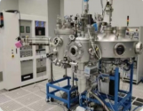
Mercury cadmium telluride molecular beam epitaxy equipment passed the technical achievement evaluation.

In order to meet the national security strategic needs, the Kunming Institute of Physics launched the project of developing mercury cadmium telluride molecular beam epitaxy equipment in 2020. It has carried out research on key control technologies such as vacuum degree, temperature, and beam current of MBE equipment, and successfully developed a 4 Inch substrate HgCdTe molecular beam epitaxy equipment. On May 15, 2023, entrusted by the Kunming Institute of Physics, the expert review team organized by the Shanghai Vacuum Society held the technical achievement appraisal of the "HgCdTe Molecular Beam Epitaxy Equipment" developed by the Kunming Institute of Physics at the Institute of Optoelectronics, Fudan University. meeting.
The appraisal committee consists of Professor Sun Zhuo from East China Normal University/Academician of Asia-Pacific Academy of Materials Science, Professor Lu Hongliang from the School of Microelectronics of Fudan University, Professor Li Xifeng from the Flat Panel Display Engineering Technology Research Center of Shanghai University, Associate Researcher Mo Xiaoliang from the Institute of Optoelectronics of Fudan University and Han Jianhua from Shanghai Vacuum Society It is composed of 5 experts including senior engineers. The Appraisal Committee listened to the report on the completion of the development of the team of researcher Wang Shanli of the Kunming Institute of Physics, and watched the video recording of the equipment. Reviewed the research and development summary report, relevant application certificates, stage acceptance form, acceptance procedures, advanced description, market situation analysis and other report materials.
After discussion by the Appraisal Committee, it is considered that the development of HgCdTe molecular beam epitaxy equipment has successfully broken the embargo of this equipment to China from abroad, and realized the first sale of similar equipment in China, with remarkable economic benefits. It can meet the domestic demand for MBE equipment in the future, fill the blank of such equipment in Yunnan Province, and strongly support the development of domestic semiconductor equipment. The technical indicators of the HgCdTe molecular beam epitaxy equipment meet the design requirements, and the equipment development level is first-class in China and has reached the international advanced level. It is suggested that this equipment be promoted in the vacuum industry and make more contributions to the realization of self-reliance and self-improvement of science and technology.
- Status
- Not open for further replies.
