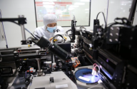
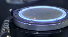
Huagong Technology has successfully developed China's first domestically-produced high-end wafer laser cutting equipment with 100% localization of core components.
According to Huang Wei, the Product Director of Huagong Laser Semiconductor, the thermal impact and kerf width of wafer mechanical cutting are about 20 micrometers, while traditional lasers achieve around 10 micrometers. However, after a year of effort, Huagong Technology has successfully upgraded its semiconductor wafer cutting technology, reducing the thermal impact to zero and decreasing the kerf size to less than 5 micrometers. The cutting line width can be achieved within 10 micrometers.
Note by ITHome: Regardless of whether wafer cutting and chip separation are done mechanically or with lasers, they will generate thermal impact and kerf due to material contact and high-speed movement, thus affecting chip performance.
It is revealed that Huagong Laser is currently developing the third-generation semiconductor wafer laser modification cutting equipment and plans to launch the new product in July this year. They are also developing the third-generation semiconductor wafer laser annealing equipment with independent intellectual property rights in China.
According to the official website of Huagong Technology, the company, originated from the renowned Chinese university Huazhong University of Science and Technology, is the "first publicly traded laser company in China." Its business encompasses intelligent manufacturing equipment supported by laser processing technology, optical interconnection and wireless connection business supported by information and communication technology, and sensor business supported by sensitive electronic technology. The company's industrial base covers an area of nearly 2,000 mu (approximately 1,333,333 square meters).


