Chinese semiconductor industry

Status
Not open for further replies.

tphuang

Lieutenant General
Staff member
Super Moderator
VIP Professional
Registered Member
Please, Log in or Register to view URLs content!
HK chief exec John Lee met with Biren recently on cooperation and supporting HK's tech development

Please, Log in or Register to view URLs content!
VP of China's law society also met with Biren, i guess China's judicial system needs AI computation also

Please, Log in or Register to view URLs content!
Meta-X joined 中电云人工智能创新应用产业联盟
so another cloud service
 

tokenanalyst

Brigadier
Registered Member

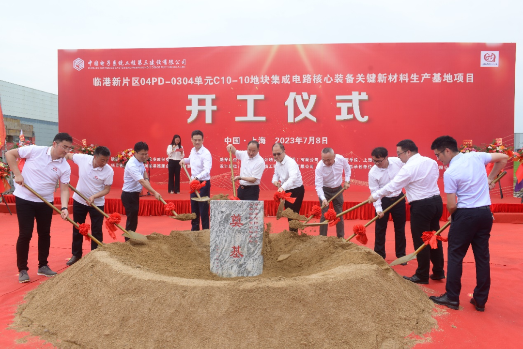
Qianghua Co., Ltd.’s key new material production base for integrated circuit core equipment started construction in Lingang Industrial Zone​

On July 8, the groundbreaking ceremony of Shanghai Qianghua Industrial Co., Ltd.'s "Integrated Circuit Core Equipment New Materials Production Base Project" was held.
883756332170.09111012066147139.9491.png

It is reported that the Lingang project of Qianghua shares is located in Lingang Industrial Zone, invested and constructed by Shanghai Qianghua Industrial Co., Ltd., and undertaken by China Electronics System Engineering Third Construction Co., Ltd. The project covers an area of 32 acres and is mainly used to produce 8-inch-12-inch high-purity, high-precision quartz devices and other related silicon-based devices. The project started construction in less than 4 months since the land acquisition in March this year.
According to the news from Shanghai Lingang Industrial Zone, Shanghai Qianghua Industrial Co., Ltd. is a private high-tech enterprise with more than 20 years of quartz processing experience, mainly engaged in the research and development, production and sales of high-purity and high-precision quartz material products. Qianghua Co., Ltd. is a key enterprise in the link of integrated circuit materials in Lingang New Area. In April 2022, Qianghua officially joined the Lingang New Area, successfully filling the blank field of quartz materials in the new area.

Please, Log in or Register to view URLs content!
 

Wahid145

Junior Member
Registered Member
Please, Log in or Register to view URLs content!

BYD has invested into Jiaxin Semiconductor, which was founded by Wanye in April 2021

Looks like Jiaxin has received 460m RMB of orders for etching & deposition equipments since 2nd half of 2022
I am a bit dubious about the Jiaxin. How come they can come up with so many equipment (almost competing with Naura at this point) in such short period of time. Mastering so many complex stuff like CVD, PVD, Etch & Rapid Heat Treatment sound a bit dramatic and reminds me of Wuhan Hongxin who were promising 7 nm eventhough the company was found literally overnight and look what happened to them.

I haven't seen Jiaxin having a long history unlike Naura, AMEC, Piotec and other old ones.
 

tokenanalyst

Brigadier
Registered Member
I am a bit dubious about the Jiaxin. How come they can come up with so many equipment (almost competing with Naura at this point) in such short period of time. Mastering so many complex stuff like CVD, PVD, Etch & Rapid Heat Treatment sound a bit dramatic and reminds me of Wuhan Hongxin who were promising 7 nm eventhough the company was found literally overnight and look what happened to them.

I haven't seen Jiaxin having a long history unlike Naura, AMEC, Piotec and other old ones.
They are part of the Wanye Group. The group that owns keystone ion implantation tools and they also own compart for manufacturing parts for semiconductor equipment and manufacturing in general, so there is already some good background. They where funded by one of SMIC ex-boss Zhang Rujing, a guy who knows of this stuff, it seems they where funded to do refurbishing of semiconductor equipment but looks like they are moving to design and manufacture their own equipment probably to fill areas that are not cover by other Chinese companies that SMIC was having trouble to find tools for their processes.​

Please, Log in or Register to view URLs content!
 

latenlazy

Brigadier
They are part of the Wanye Group. The group that owns keystone ion implantation tools and they also own compart for manufacturing parts for semiconductor equipment and manufacturing in general, so there is already some good background. They where funded by one of SMIC ex-boss Zhang Rujing, a guy who knows of this stuff, it seems they where funded to do refurbishing of semiconductor equipment but looks like they are moving to design and manufacture their own equipment probably to fill areas that are not cover by other Chinese companies that SMIC was having trouble to find tools for their processes.​

Please, Log in or Register to view URLs content!
And just for the record moving from an equipment servicing business to making one’s own in-house design is not an uncommon path for capital equipment providers. It teaches you all the business support operations before you’ve committed the higher capital to make your own designs and set up your own production.
 

caudaceus

Senior Member
Registered Member
View attachment 115692

Web series will be telecast regarding China's indigenous lithography machine. they specially mentioned DUVi. interesting

Youku Studio recently announced that the online drama "My China Core" is scheduled to start broadcasting on July 10.

Storyline -

A private technology company undertakes the scientific research project of the National Burning Point Program, and develops 193nm DUV lasers for lithography machines. The lithography machine using this laser can solve the production problems of most advanced integrated circuit chips.

In order to make progress in scientific research and realize the dream in his heart, Li Weiguo led Yu Lan and He Zhangci to challenge the difficult scientific research difficulties together.

*******************************************************************************************
without approval from higher authority they couldn't produce such a web series on this sensitive technology. another solid Hint about China's progress in Lithography sector.
Me : Mom I want to watch Oppenheimer
Mom : We have Oppenheimer at home

Oppenheimer at home :
 

tokenanalyst

Brigadier
Registered Member
VeriSilicon stated that in terms of advanced semiconductor process nodes, the company already has successful tape-out experience of 14nm/10nm/7nm/5nm FinFET and 28nm/22nm FD-SOI process node chips, and currently has multiple 5nm design projects The tape-out is completed, and multiple design projects are waiting for tape-out. Among the chip design projects implemented by the company, the 14nm and below process node projects are mainly distributed in data centers, Internet of Things and other fields. With the smooth development of the above customer projects, they will gradually enter the mass production stage and continue to contribute revenue.

Please, Log in or Register to view URLs content!
 

tphuang

Lieutenant General
Staff member
Super Moderator
VIP Professional
Registered Member
I did a little research on Innoscience given the recent Gallium news. I do think part of rationale is sanctioning Gallium export is to also help firms like Innoscience to dominate the GaN supply chain. Beating their competitors (pretty much everyone in America)

when Innoscience started, they directly moved toward producing 8-inch GaN-on-Si wafers and products when everyone else was at 6-inch.

The reason is the lower cost & higher production potential of 8-inch.

They started off with a small production line in Zhuhai able to produce just 4k wpm, but has a second one in Suzhou they are building with goal of hitting max capacity of 65k wpm by 2025!!!! (that's humongous since most other fabs are just a few thousand 6-inch wpm right now)

Please, Log in or Register to view URLs content!
This page is really good. It shows them having a full range of product from 15V-700V (anything higher than this typically is better with SiC). Their product will be used in data centers, RF products, chargers, Lidars, smart music, tv and such.

Right now, suzhou plant is just at 7k wpm and they are probably already the largest player.

It has shipped 120 million GaN product by early this year & was the first in the industry to hit 100 million unit at end of last year
Please, Log in or Register to view URLs content!
Notice how there it mentioned of product from 30-150V and 650V? Looks like within a few months, I managed to develop 15V and 700V. So they definitely are continuing to innovate pretty quickly.

And they want to get into EVs by 2024. They are looking into where GaN can be used in EVs
Please, Log in or Register to view URLs content!
另外,在电动汽车应用领域,英诺赛科珠海工厂已通过汽车认证,预计将在2024年生产用于汽车应用的8英寸硅基GaN器件。目前,珠海工厂GaN晶圆月产能为4000片,到2025年,珠海和苏州两大基地的月产能预计可达70000片左右。

目前,国内已有顶级车载激光雷达客户采用了英诺赛科的GaN器件。除此之外,英诺赛科也已开始联合国内及韩国的大型Tier 1厂商共同研发GaN车用项目。
 
Status
Not open for further replies.
Top